SBAS650C May 2014 – April 2021 AFE4403
PRODUCTION DATA
- 1 Features
- 2 Applications
- 3 Description
- 4 Revision History
- 5 Device Family Options
- 6 Pin Configuration and Functions
- 7 Specifications
- 8 Detailed Description
- 9 Application Information Disclaimer
- 10Power Supply Recommendations
- 11Layout
- 12Device and Documentation Support
- 13Mechanical, Packaging, and Orderable Information
Package Options
Mechanical Data (Package|Pins)
- YZP|36
Thermal pad, mechanical data (Package|Pins)
Orderable Information
8.3.3.1 Using the Timer Module
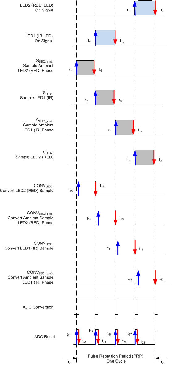
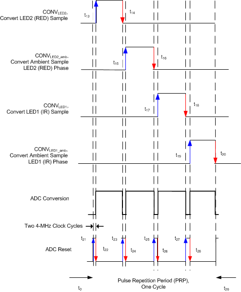
The timer module registers can be used to program the start and end instants in units of 4-MHz clock cycles. These timing instants and the corresponding registers are listed in Table 8-2.
Note that the device does not restrict the values in these registers; thus, the start and end edges can be positioned anywhere within the pulse repetition period. Care must be taken by the user to program suitable values in these registers to avoid overlapping the signals and to make sure none of the edges exceed the value programmed in the PRP register. Writing the same value in the start and end registers results in a pulse duration of one clock cycle. The following steps describe the timer sequencing configuration:
- With respect to the start of the PRP period (indicated by timing instant t0 in Figure 8-13), the following sequence of conversions must be followed in order: convert LED2 → LED2 ambient → LED1 → LED1 ambient.
- Also, starting from t0, the sequence of sampling instants must be staggered with respect to the respective conversions as follows: sample LED2 ambient → LED1 → LED1 ambient → LED2.
- Finally, align the edges for the two LED pulses with the respective sampling instants.
| TIME INSTANT (See Figure 8-13 and Figure 8-14)(3) | DESCRIPTION | CORRESPONDING REGISTER ADDRESS AND REGISTER BITS | EXAMPLE(1) (Decimal) |
|---|---|---|---|
| t0 | Start of pulse repetition period | No register control | — |
| t1 | Start of sample LED2 pulse | LED2STC[15:0], register 01h | 6050 |
| t2 | End of sample LED2 pulse | LED2ENDC[15:0], register 02h | 7998 |
| t3 | Start of LED2 pulse | LED2LEDSTC[15:0], register 03h | 6000 |
| t4 | End of LED2 pulse | LED2LEDENDC[15:0], register 04h | 7999 |
| t5 | Start of sample LED2 ambient pulse | ALED2STC[15:0], register 05h | 50 |
| t6 | End of sample LED2 ambient pulse | ALED2ENDC[15:0], register 06h | 1998 |
| t7 | Start of sample LED1 pulse | LED1STC[15:0], register 07h | 2050 |
| t8 | End of sample LED1 pulse | LED1ENDC[15:0], register 08h | 3998 |
| t9 | Start of LED1 pulse | LED1LEDSTC[15:0], register 09h | 2000 |
| t10 | End of LED1 pulse | LED1LEDENDC[15:0], register 0Ah | 3999 |
| t11 | Start of sample LED1 ambient pulse | ALED1STC[15:0], register 0Bh | 4050 |
| t12 | End of sample LED1 ambient pulse | ALED1ENDC[15:0], register 0Ch | 5998 |
| t13 | Start of convert LED2 pulse | LED2CONVST[15:0], register 0Dh Must start one AFE clock cycle after the ADC reset pulse ends. | 4 |
| t14 | End of convert LED2 pulse | LED2CONVEND[15:0], register 0Eh | 1999 |
| t15 | Start of convert LED2 ambient pulse | ALED2CONVST[15:0], register 0Fh Must start one AFE clock cycle after the ADC reset pulse ends. | 2004 |
| t16 | End of convert LED2 ambient pulse | ALED2CONVEND[15:0], register 10h | 3999 |
| t17 | Start of convert LED1 pulse | LED1CONVST[15:0], register 11h Must start one AFE clock cycle after the ADC reset pulse ends. | 4004 |
| t18 | End of convert LED1 pulse | LED1CONVEND[15:0], register 12h | 5999 |
| t19 | Start of convert LED1 ambient pulse | ALED1CONVST[15:0], register 13h Must start one AFE clock cycle after the ADC reset pulse ends. | 6004 |
| t20 | End of convert LED1 ambient pulse | ALED1CONVEND[15:0], register 14h | 7999 |
| t21 | Start of first ADC conversion reset pulse | ADCRSTSTCT0[15:0], register 15h | 0 |
| t22 | End of first ADC conversion reset pulse(2) | ADCRSTENDCT0[15:0], register 16h | 3 |
| t23 | Start of second ADC conversion reset pulse | ADCRSTSTCT1[15:0], register 17h | 2000 |
| t24 | End of second ADC conversion reset pulse(2) | ADCRSTENDCT1[15:0], register 18h | 2003 |
| t25 | Start of third ADC conversion reset pulse | ADCRSTSTCT2[15:0], register 19h | 4000 |
| t26 | End of third ADC conversion reset pulse(2) | ADCRSTENDCT2[15:0], register 1Ah | 4003 |
| t27 | Start of fourth ADC conversion reset pulse | ADCRSTSTCT3[15:0], register 1Bh | 6000 |
| t28 | End of fourth ADC conversion reset pulse(2) | ADCRSTENDCT3[15:0], register 1Ch | 6003 |
| t29 | End of pulse repetition period | PRPCOUNT[15:0], register 1Dh | 7999 |

