SBAS650C May 2014 – April 2021 AFE4403
PRODUCTION DATA
- 1 Features
- 2 Applications
- 3 Description
- 4 Revision History
- 5 Device Family Options
- 6 Pin Configuration and Functions
- 7 Specifications
- 8 Detailed Description
- 9 Application Information Disclaimer
- 10Power Supply Recommendations
- 11Layout
- 12Device and Documentation Support
- 13Mechanical, Packaging, and Orderable Information
Package Options
Mechanical Data (Package|Pins)
- YZP|36
Thermal pad, mechanical data (Package|Pins)
Orderable Information
8.3.1.1 Receiver Front-End
The receiver consists of a differential current-to-voltage (I-V) transimpedance amplifier (TIA) that converts the input photodiode current into an appropriate voltage, as shown in Figure 8-1. The feedback resistor of the amplifier (RF) is programmable to support a wide range of photodiode currents. Available RF values include:
1 MΩ, 500 kΩ, 250 kΩ, 100 kΩ, 50 kΩ, 25 kΩ, and 10 kΩ.
The device is ideally suited as a front-end for a PPG (photoplethysmography) application. In such an application, the light from the LED is reflected (or transmitted) from (or through) the various components inside the body (such as blood, tissue, and so forth) and are received by the photodiode. The signal received by the photodiode has three distinct components:
- A pulsatile or ac component that arises as a result of the changes in blood volume through the arteries.
- A constant dc signal that is reflected or transmitted from the time invariant components in the path of light. This constant dc component is referred to as the pleth signal.
- Ambient light entering the photodiode.
 Figure 8-1 Receiver Front-End
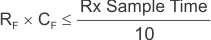
The RF amplifier and the feedback capacitor (CF) form a low-pass filter for the input signal current. Always ensure that the low-pass filter RC time constant has sufficiently high bandwidth (as shown by Equation 1) because the input current consists of pulses. For this reason, the feedback capacitor is also programmable. Available CF values include: 5 pF, 10 pF, 25 pF, 50 pF, 100 pF, and 250 pF. Any combination of these capacitors can also be used.
The output voltage of the I-V amplifier includes the pleth component (the desired signal) and a component resulting from the ambient light leakage. The I-V amplifier is followed by the second stage, which consists of a current digital-to-analog converter (DAC) that sources the cancellation current and an amplifier that gains up the pleth component alone. The amplifier has five programmable gain settings: 0 dB, 3.5 dB, 6 dB, 9.5 dB, and 12 dB. The gained-up pleth signal is then low-pass filtered (500-Hz bandwidth) and buffered before driving a 22-bit ADC. The current DAC has a cancellation current range of 10 µA with 10 steps (1 µA each). The DAC value can be digitally specified with the SPI interface. Using ambient compensation with the ambient DAC allows the dc-biased signal to be centered to near mid-point of the amplifier (±0.9 V). Using the gain of the second stage allows for more of the available ADC dynamic range to be used.
The output of the ambient cancellation amplifier is separated into LED2 and LED1 channels. When LED2 is on, the amplifier output is filtered and sampled on capacitor CLED2. Similarly, the LED1 signal is sampled on the CLED1 capacitor when LED1 is on. In between the LED2 and LED1 pulses, the idle amplifier output is sampled to estimate the ambient signal on capacitors CLED2_amb and CLED1_amb.
The sampling duration is termed the Rx sample time and is programmable for each signal, independently. The sampling can start after the I-V amplifier output is stable (to account for LED and cable settling times). The Rx sample time is used for all dynamic range calculations; the minimum time recommended is 50 µs. While the AFE4403 can support pulse widths lower than 50 us, having too low a pulse width could result in a degraded signal and noise from the photodiode.
A single, 22-bit ADC converts the sampled LED2, LED1, and ambient signals sequentially. Each conversion provides a single digital code at the ADC output. As discussed in the Receiver Timing section, the conversions are meant to be staggered so that the LED2 conversion starts after the end of the LED2 sample phase, and so on.
Note that four data streams are available at the ADC output (LED2, LED1, ambient LED2, and ambient LED1) at the same rate as the pulse repetition frequency. The ADC is followed by a digital ambient subtraction block that additionally outputs the (LED2 – ambient LED2) and (LED1 – ambient LED1) data values.
The model of the photodiode and the connection to the TIA is shown in Figure 8-2.
 Figure 8-2 TIA Block Diagram
Iin is the signal current generated by the photodiode in response to the incident light. Cin is the zero-bias capacitance of the photodiode. The current-to-voltage gain in the TIA is given by Equation 2:
For example, for a photodiode current of Iin = 1 µA and a TIA gain setting of RF = 100 kΩ, the differential output of the TIA is equal to 200 mV. The TIA has an operating range of ±1 V, and the ADC has an input full-scale range of ±1.2 V (the extra margin is to prevent the ADC from saturating while operating the TIA at the fullest output range). Furthermore, because the PPG signal is one-sided, only one half of the full-scale is used. TI recommends operating the device at a dc level that is not more than 50% to 60% of the ADC full-scale. The margin allows for sudden changes in the signal level that might saturate the signal chain if operating too close to full-scale. Signal levels are shown in Figure 8-3:
 Figure 8-3 Signal Levels in TIA and ADC
On startup, a gain calibration algorithm running on the microcontroller unit (MCU) can be used to monitor the dc level and adjusts the LED current and TIA gain to get close to the target dc level. In addition to a target dc level, a high and low threshold (for example 80% and 20% of full-scale) can be determined that can cause the algorithm to switch to a different TIA gain or LED current setting when the signal amplitude changes beyond these thresholds.
In heart rate monitoring (HRM) applications demanding small-form factors, the sensor size can be so small (and the signal currents so low) that they do not occupy even 50% of full-scale even with the highest TIA gain setting of 1 MΩ, which is the case for signal currents that are less than 300 nA. As such, experimentation with various use cases is essential in order to determine the optimal target value, as well as high and low thresholds. Also, by enabling the stage 2 and introducing additional gain (up to 12 dB), a few extra decibels of SNR can be achieved.