SLUSD20B july 2018 – april 2023 BQ25710
PRODUCTION DATA
- 1 Features
- 2 Applications
- 3 Description
- 4 Revision History
- 5 Description (continued)
- 6 Device Comparison Table
- 7 Pin Configuration and Functions
- 8 Specifications
-
9 Detailed Description
- 9.1 Overview
- 9.2 Functional Block Diagram
- 9.3
Feature Description
- 9.3.1 Power-Up from Battery Without DC Source
- 9.3.2 Vmin Active Protection (VAP) when Battery only Mode
- 9.3.3 Power-Up From DC Source
- 9.3.4 USB On-The-Go (OTG)
- 9.3.5 Converter Operation
- 9.3.6 Current and Power Monitor
- 9.3.7 Input Source Dynamic Power Manage
- 9.3.8 Two-Level Adapter Current Limit (Peak Power Mode)
- 9.3.9 Processor Hot Indication
- 9.3.10
Device Protection
- 9.3.10.1 Watchdog Timer
- 9.3.10.2 Input Overvoltage Protection (ACOV)
- 9.3.10.3 Input Overcurrent Protection (ACOC)
- 9.3.10.4 System Overvoltage Protection (SYSOVP)
- 9.3.10.5 Battery Overvoltage Protection (BATOVP)
- 9.3.10.6 Battery Short
- 9.3.10.7 System Short Hiccup Mode
- 9.3.10.8 Thermal Shutdown (TSHUT)
- 9.4 Device Functional Modes
- 9.5 Programming
- 9.6
Register Map
- 9.6.1
Setting Charge and
PROCHOT Options
- 9.6.1.1 ChargeOption0 Register (SMBus address = 12h) [reset = E70Eh]
- 9.6.1.2 ChargeOption1 Register (SMBus address = 30h) [reset = 0211h]
- 9.6.1.3 ChargeOption2 Register (SMBus address = 31h) [reset = 02B7h]
- 9.6.1.4 ChargeOption3 Register (SMBus address = 32h) [reset = 0030h]
- 9.6.1.5 ProchotOption0 Register (SMBus address = 33h) [reset = 4A65h]
- 9.6.1.6 ProchotOption1 Register (SMBus address = 34h) [reset = 81A0h]
- 9.6.1.7 ADCOption Register (SMBus address = 35h) [reset = 2000h]
- 9.6.2 Charge and PROCHOT Status
- 9.6.3 ChargeCurrent Register (SMBus address = 14h) [reset = 0000h]
- 9.6.4 MaxChargeVoltage Register (SMBus address = 15h) [reset value based on CELL_BATPRESZ pin setting]
- 9.6.5 MinSystemVoltage Register (SMBus address = 3Eh) [reset value based on CELL_BATPRESZ pin setting]
- 9.6.6 Input Current and Input Voltage Registers for Dynamic Power Management
- 9.6.7 OTGVoltage Register (SMBus address = 3Bh) [reset = 0000h]
- 9.6.8 OTGCurrent Register (SMBus address = 3Ch) [reset = 0000h]
- 9.6.9 ADCVBUS/PSYS Register (SMBus address = 23h)
- 9.6.10 ADCIBAT Register (SMBus address = 24h)
- 9.6.11 ADCIINCMPIN Register (SMBus address = 25h)
- 9.6.12 ADCVSYSVBAT Register (SMBus address = 26h)
- 9.6.13 ID Registers
- 9.6.1
Setting Charge and
PROCHOT Options
- 10Application and Implementation
- 11Power Supply Recommendations
- 12Layout
- 13Device and Documentation Support
- 14Mechanical, Packaging, and Orderable Information
Package Options
Mechanical Data (Package|Pins)
- RSN|32
Thermal pad, mechanical data (Package|Pins)
- RSN|32
Orderable Information
10.2.2.5 Power MOSFETs Selection
Four external N-channel MOSFETs are used for a synchronous switching battery charger. The gate drivers are internally integrated into the IC with 6 V of gate drive voltage. 30 V or higher voltage rating MOSFETs are preferred for 19 V - 20 V input voltage.
Figure-of-merit (FOM) is usually used for selecting proper MOSFET based on a tradeoff between the conduction loss and switching loss. For the top side MOSFET, FOM is defined as the product of a MOSFET's on-resistance, RDS(ON), and the gate-to-drain charge, QGD. For the bottom side MOSFET, FOM is defined as the product of the MOSFET's on-resistance, RDS(ON), and the total gate charge, QG.
The lower the FOM value, the lower the total power loss. Usually lower RDS(ON) has higher cost with the same package size.
The top-side MOSFET loss includes conduction loss and switching loss. It is a function of duty cycle (D=VOUT/VIN), charging current (ICHG), MOSFET's on-resistance (RDS(ON)), input voltage (VIN), switching frequency (fS), turn on time (ton) and turn off time (toff):

The first item represents the conduction loss. Usually MOSFET RDS(ON) increases by 50% with 100°C junction temperature rise. The second term represents the switching loss. The MOSFET turn-on and turn-off times are given by:
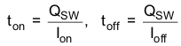
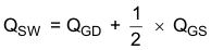
where Qsw is the switching charge, Ion is the turn-on gate driving current and Ioff is the turn-off gate driving current. If the switching charge is not given in MOSFET datasheet, it can be estimated by gate-to-drain charge (QGD) and gate-to-source charge (QGS):
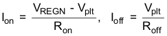
Gate driving current can be estimated by REGN voltage (VREGN), MOSFET plateau voltage (Vplt), total turn-on gate resistance (Ron) and turn-off gate resistance (Roff) of the gate driver:
The conduction loss of the bottom-side MOSFET is calculated with the following equation when it operates in synchronous continuous conduction mode:
When charger operates in non-synchronous mode, the bottom-side MOSFET is off. As a result all the freewheeling current goes through the body-diode of the bottom-side MOSFET. The body diode power loss depends on its forward voltage drop (VF), non-synchronous mode charging current (INONSYNC), and duty cycle (D).
The maximum charging current in non-synchronous mode can be up to 0.25 A for a 10-mΩ charging current sensing resistor or 0.5 A if battery voltage is below 2.5 V. The minimum duty cycle happens at lowest battery voltage. Choose the bottom-side MOSFET with either an internal Schottky or body diode capable of carrying the maximum non-synchronous mode charging current.