SLUSD20B july 2018 – april 2023 BQ25710
PRODUCTION DATA
- 1 Features
- 2 Applications
- 3 Description
- 4 Revision History
- 5 Description (continued)
- 6 Device Comparison Table
- 7 Pin Configuration and Functions
- 8 Specifications
-
9 Detailed Description
- 9.1 Overview
- 9.2 Functional Block Diagram
- 9.3
Feature Description
- 9.3.1 Power-Up from Battery Without DC Source
- 9.3.2 Vmin Active Protection (VAP) when Battery only Mode
- 9.3.3 Power-Up From DC Source
- 9.3.4 USB On-The-Go (OTG)
- 9.3.5 Converter Operation
- 9.3.6 Current and Power Monitor
- 9.3.7 Input Source Dynamic Power Manage
- 9.3.8 Two-Level Adapter Current Limit (Peak Power Mode)
- 9.3.9 Processor Hot Indication
- 9.3.10
Device Protection
- 9.3.10.1 Watchdog Timer
- 9.3.10.2 Input Overvoltage Protection (ACOV)
- 9.3.10.3 Input Overcurrent Protection (ACOC)
- 9.3.10.4 System Overvoltage Protection (SYSOVP)
- 9.3.10.5 Battery Overvoltage Protection (BATOVP)
- 9.3.10.6 Battery Short
- 9.3.10.7 System Short Hiccup Mode
- 9.3.10.8 Thermal Shutdown (TSHUT)
- 9.4 Device Functional Modes
- 9.5 Programming
- 9.6
Register Map
- 9.6.1
Setting Charge and
PROCHOT Options
- 9.6.1.1 ChargeOption0 Register (SMBus address = 12h) [reset = E70Eh]
- 9.6.1.2 ChargeOption1 Register (SMBus address = 30h) [reset = 0211h]
- 9.6.1.3 ChargeOption2 Register (SMBus address = 31h) [reset = 02B7h]
- 9.6.1.4 ChargeOption3 Register (SMBus address = 32h) [reset = 0030h]
- 9.6.1.5 ProchotOption0 Register (SMBus address = 33h) [reset = 4A65h]
- 9.6.1.6 ProchotOption1 Register (SMBus address = 34h) [reset = 81A0h]
- 9.6.1.7 ADCOption Register (SMBus address = 35h) [reset = 2000h]
- 9.6.2 Charge and PROCHOT Status
- 9.6.3 ChargeCurrent Register (SMBus address = 14h) [reset = 0000h]
- 9.6.4 MaxChargeVoltage Register (SMBus address = 15h) [reset value based on CELL_BATPRESZ pin setting]
- 9.6.5 MinSystemVoltage Register (SMBus address = 3Eh) [reset value based on CELL_BATPRESZ pin setting]
- 9.6.6 Input Current and Input Voltage Registers for Dynamic Power Management
- 9.6.7 OTGVoltage Register (SMBus address = 3Bh) [reset = 0000h]
- 9.6.8 OTGCurrent Register (SMBus address = 3Ch) [reset = 0000h]
- 9.6.9 ADCVBUS/PSYS Register (SMBus address = 23h)
- 9.6.10 ADCIBAT Register (SMBus address = 24h)
- 9.6.11 ADCIINCMPIN Register (SMBus address = 25h)
- 9.6.12 ADCVSYSVBAT Register (SMBus address = 26h)
- 9.6.13 ID Registers
- 9.6.1
Setting Charge and
PROCHOT Options
- 10Application and Implementation
- 11Power Supply Recommendations
- 12Layout
- 13Device and Documentation Support
- 14Mechanical, Packaging, and Orderable Information
Package Options
Mechanical Data (Package|Pins)
- RSN|32
Thermal pad, mechanical data (Package|Pins)
- RSN|32
Orderable Information
10.2.2.1 ACP-ACN Input Filter
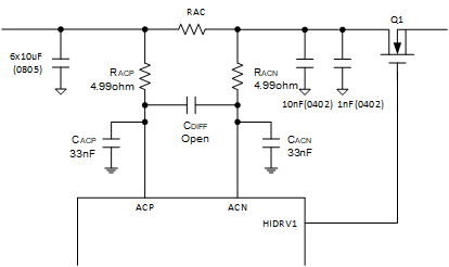
The BQ25710 has average current mode control. The input current sensing through ACP/ACN is critical to recover inductor current ripple. Parasitic inductance on board will generate high frequency ringing on ACP-ACN which overwhelms converter sensed inductor current information, so it is difficult to manage parasitic inductance created based on different PCB layout. Bigger parasitic inductance will generate bigger sense current ringing which will cause the average current control loop to go into oscillation.
For real system board condition, we suggest to use below circuit design to get best result and filter noise induced from different PCB parasitic factor. With time constant of filter from 47 nsec to 200 nsec, the filtering on ringing is effective and in the meantime, the delay of on the sensed signal is small and therefore poses no concern for average current mode control.
 Figure 10-2 ACN-ACP Input
Filter