SNVS671F February   2011  – May 2019 LM21212-1

PRODUCTION DATA.  

  1. Features
  2. Applications
  3. Description
    1.     Device Images
      1.      Simplified Application Circuit
  4. Revision History
  5. Description
  6. Pin Configuration and Functions
    1.     Pin Functions
  7. Specifications
    1. 7.1 Absolute Maximum Ratings
    2. 7.2 ESD Ratings
    3. 7.3 Recommended Operating Conditions
    4. 7.4 Thermal Information
    5. 7.5 Electrical Characteristics
    6. 7.6 Typical Performance Characteristics
  8. Detailed Description
    1. 8.1 Overview
    2. 8.2 Functional Block Diagram
    3. 8.3 Feature Description
      1. 8.3.1 Frequency Synchronization
      2. 8.3.2 Precision Enable
      3. 8.3.3 UVLO
      4. 8.3.4 Current Limit
      5. 8.3.5 Short-Circuit Protection
      6. 8.3.6 Thermal Protection
      7. 8.3.7 Power-Good Flag
      8. 8.3.8 Light Load Operation
  9. Application and Implementation
    1. 9.1 Application Information
    2. 9.2 Typical Application
      1. 9.2.1 Detailed Design Procedure
        1. 9.2.1.1 Custom Design With WEBENCH® Tools
        2. 9.2.1.2 Output Voltage
        3. 9.2.1.3 Precision Enable
        4. 9.2.1.4 Soft Start
        5. 9.2.1.5 Inductor Selection
        6. 9.2.1.6 Output Capacitor Selection
        7. 9.2.1.7 Input Capacitor Selection
        8. 9.2.1.8 Control Loop Compensation
      2. 9.2.2 Application Curves
  10. 10Layout
    1. 10.1 Pcb Layout Considerations
    2. 10.2 Thermal Considerations
  11. 11Device and Documentation Support
    1. 11.1 Device Support
      1. 11.1.1 Third-Party Products Disclaimer
      2. 11.1.2 Development Support
        1. 11.1.2.1 Custom Design With Webench® Tools
    2. 11.2 Receiving Notification Of Documentation Updates
    3. 11.3 Community Resources
    4. 11.4 Trademarks
    5. 11.5 Electrostatic Discharge Caution
    6. 11.6 Glossary
  12. 12Mechanical, Packaging, And Orderable Information

Package Options

Mechanical Data (Package|Pins)
Thermal pad, mechanical data (Package|Pins)
Orderable Information

Frequency Synchronization

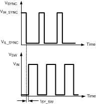
The sync (SYNC) pin allows the LM21212-1 to be switched at an external clock frequency. When a clock signal is present on the SYNC pin within the allowable frequency range, 300 kHz to 1.5 MHz, the device will synchronize the turn-on of the high side FET (switch rising) to the negative edge of the clock signal, as seen in Figure 22 . If no clock signal is present, the LM21212-1 will default to a switching frequency of 1 MHz. The clock signal can be present on the SYNC pin before the device is powered on with no loading on the clock signal. Alternatively, if no clock is present while the device is powered up, it will begin switching at the default frequency of 1 MHz. Once the clock signal is present, the device will begin synchronizing to the clock frequency. The length of time necessary for the synchronization depends on the clock frequency.
LM21212-1 30119933.gifFigure 22. Frequency Synchronization