SNVS671F February 2011 – May 2019 LM21212-1
PRODUCTION DATA.
- 1 Features
- 2 Applications
- 3 Description
- 4 Revision History
- 5 Description
- 6 Pin Configuration and Functions
- 7 Specifications
- 8 Detailed Description
- 9 Application and Implementation
- 10Layout
- 11Device and Documentation Support
- 12Mechanical, Packaging, And Orderable Information
Package Options
Mechanical Data (Package|Pins)
- PWP|20
Thermal pad, mechanical data (Package|Pins)
- PWP|20
Orderable Information
10.2 Thermal Considerations
The thermal characteristics of the LM21212-1 are specified using the parameter θJA, which relates the junction temperature to the ambient temperature. Although the value of θJA is dependant on many variables, it still can be used to approximate the operating junction temperature of the device.
To obtain an estimate of the device junction temperature, one may use the following relationship:

and

Where:
TJ is the junction temperature in °C, PIN is the input power in Watts (PIN = VIN x IIN), θJA is the junction to ambient thermal resistance for the LM21212-1, TA is the ambient temperature in °C, and IOUT is the output load current.
It is important to always keep the operating junction temperature (TJ) below 125°C for reliable operation. If the junction temperature exceeds 165°C the device will cycle in and out of thermal shutdown. If thermal shutdown occurs it is a sign of inadequate heatsinking or excessive power dissipation in the device.
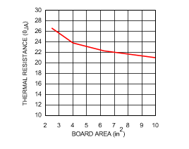
Figure 40, shown below, provides a better approximation of the θJA for a given PCB copper area. The PCB used in this test consisted of 4 layers: 1oz. copper was used for the internal layers while the external layers were plated to 2oz. copper weight. To provide an optimal thermal connection, a 3 x 4 array of 8 mil. vias under the thermal pad were used, and an additional sixteen 8 mil. vias under the rest of the device were used to connect the 4 layers.
 Figure 40. Thermal Resistance vs PCB Area (4 Layer Board)
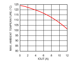
 Figure 41 shows a plot of the maximum ambient temperature vs output current for the typical application circuit shown in Figure 38, assuming a θJA value of 24°C/W.
 Figure 41. Maximum Ambient Temperature vs Output Current (0 LFM)