SCLS374P May 1997 – April 2024 SN74AHCT595
PRODMIX
- 1
- 1 Features
- 2 Applications
- 3 Description
- 4 Pin Configuration and Functions
- 5 Specifications
- 6 Parameter Measurement Information
- 7 Detailed Description
- 8 Application and Implementation
- 9 Device and Documentation Support
- 10Revision History
- 11Mechanical, Packaging, and Orderable Information
Package Options
Refer to the PDF data sheet for device specific package drawings
Mechanical Data (Package|Pins)
- BQB|16
- DB|16
- PW|16
- N|16
- D|16
Thermal pad, mechanical data (Package|Pins)
Orderable Information
4 Pin Configuration and Functions
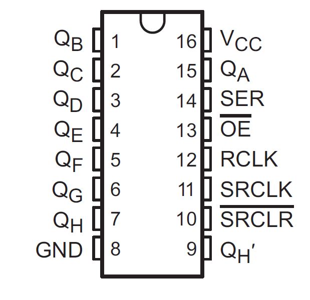
 Figure 4-1
 SN74AHCT595-Q1 PW Package (Top View)
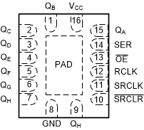
 Figure 4-2 BQB Package, 16-Pin WQFN
(Top View)
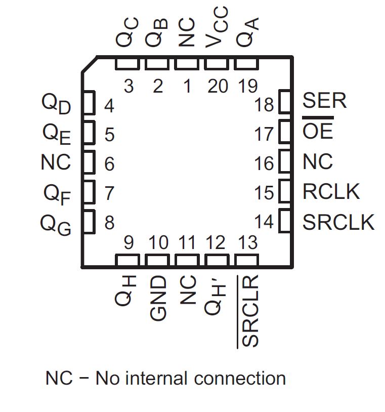
 Figure 4-3 SN74AHCT595-Q1 BQB Package (Top View)
Table 4-1 Pin Functions
| PIN | TYPE(1) | DESCRIPTION | |||
|---|---|---|---|---|---|
| NAME | SN74AHCT595 | ||||
PW |
BQB | ||||
| GND | 8 | 8 | — | Ground Pin | |
| OE | 13 | 13 | I | Output Enable | |
| QA | 15 | 15 | O | QA Output | |
| QB | 1 | 1 | O | QB Output | |
| QC | 2 | 2 | O | QC Output | |
| QD | 3 | 3 | O | QD Output | |
| QE | 4 | 4 | O | QE Output | |
| QF | 5 | 5 | O | QF Output | |
| QG | 6 | 6 | O | QG Output | |
| QH | 7 | 7 | O | QH Output | |
| QH' | 9 | 9 | O | QH' Output | |
| RCLK | 12 | 12 | I | RCLK Input | |
| SER | 14 | 14 | I | SER Input | |
| SRCLK | 11 | 11 | I | SRCLK Input | |
| SRCLR | 10 | 10 | I | SRCLR Input | |
| NC | — | — | No Connection | ||
| VCC | 16 | 16 | — | Power Pin | |
(1) I = input, O = output