SLOS930B November   2015  – November 2019 THS4541-Q1

PRODUCTION DATA.  

  1. Features
  2. Applications
  3. Description
    1.     Device Images
      1.      Simplified Schematic
      2.      Single to Differential Gain of 2, 2-VPP Output
  4. Revision History
  5. Device Comparison Table
  6. Pin Configuration and Functions
    1.     Pin Functions
  7. Specifications
    1. 7.1 Absolute Maximum Ratings
    2. 7.2 ESD Ratings
    3. 7.3 Recommended Operating Conditions
    4. 7.4 Thermal Information
    5. 7.5 Electrical Characteristics: (Vs+) – Vs– = 5 V
    6. 7.6 Electrical Characteristics: (Vs+) – Vs– = 3 V
    7. 7.7 Typical Characteristics
      1. 7.7.1 5-V Single Supply
      2. 7.7.2 3-V Single Supply
      3. 7.7.3 3-V to 5-V Supply Range
  8. Parameter Measurement Information
    1. 8.1 Example Characterization Circuits
    2. 8.2 Frequency-Response Shape Factors
    3. 8.3 I/O Headroom Considerations
    4. 8.4 Output DC Error and Drift Calculations and the Effect of Resistor Imbalances
    5. 8.5 Noise Analysis
    6. 8.6 Factors Influencing Harmonic Distortion
    7. 8.7 Driving Capacitive Loads
    8. 8.8 Thermal Analysis
  9. Detailed Description
    1. 9.1 Overview
      1. 9.1.1 Terminology and Application Assumptions
    2. 9.2 Functional Block Diagram
    3. 9.3 Feature Description
      1. 9.3.1 Differential I/O
      2. 9.3.2 Power-Down Control Pin (PD)
        1. 9.3.2.1 Operating the Power Shutdown Feature
      3. 9.3.3 Input Overdrive Operation
    4. 9.4 Device Functional Modes
      1. 9.4.1 Operation from Single-Ended Sources to Differential Outputs
        1. 9.4.1.1 AC-Coupled Signal Path Considerations for Single-Ended Input to Differential Output Conversion
        2. 9.4.1.2 DC-Coupled Input Signal Path Considerations for Single-Ended to Differential Conversion
        3. 9.4.1.3 Resistor Design Equations for the Single-Ended to Differential Configuration of the FDA
        4. 9.4.1.4 Input Impedance for the Single-Ended to Differential FDA Configuration
      2. 9.4.2 Differential-Input to Differential-Output Operation
        1. 9.4.2.1 AC-Coupled, Differential-Input to Differential-Output Design Issues
        2. 9.4.2.2 DC-Coupled, Differential-Input to Differential-Output Design Issues
  10. 10Application and Implementation
    1. 10.1 Application Information
    2. 10.2 Typical Applications
      1. 10.2.1 Designing Attenuators
        1. 10.2.1.1 Design Requirements
        2. 10.2.1.2 Detailed Design Procedure
        3. 10.2.1.3 Application Curve
      2. 10.2.2 Interfacing to High-Performance ADCs
        1. 10.2.2.1 Design Requirements
        2. 10.2.2.2 Detailed Design Procedure
        3. 10.2.2.3 Application Curve
  11. 11Power Supply Recommendations
  12. 12Layout
    1. 12.1 Layout Guidelines
    2. 12.2 Layout Example
  13. 13Device and Documentation Support
    1. 13.1 Device Support
      1. 13.1.1 Development Support
        1. 13.1.1.1 TINA Simulation Model Features
    2. 13.2 Documentation Support
      1. 13.2.1 Related Documentation
    3. 13.3 Receiving Notification of Documentation Updates
    4. 13.4 Support Resources
    5. 13.5 Trademarks
    6. 13.6 Electrostatic Discharge Caution
    7. 13.7 Glossary
  14. 14Mechanical, Packaging, and Orderable Information

Package Options

Mechanical Data (Package|Pins)
Thermal pad, mechanical data (Package|Pins)
Orderable Information

3-V Single Supply

at Vs+ = 3 V, Vs– = GND, Vocm is open, 50-Ω single-ended input to differential output, gain = 2 V/V, Rload = 500 Ω, and TA ≈ 25°C (unless otherwise noted)
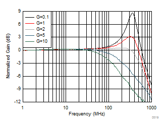
THS4541-Q1 D019_SLOS375.gif
Rf = 402 Ω, Vout = 100 mVPP, see Figure 61 and Table 6 for resistor values
Figure 19. Small-Signal Frequency Response vs Gain
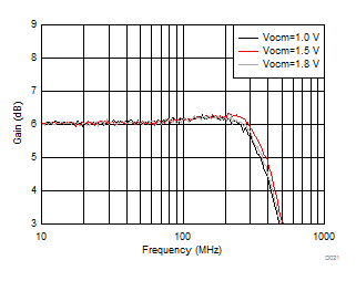
THS4541-Q1 D021_SLOS375.gif
Vout = 100 mVPP, see Figure 61 with Vocm adjusted
Figure 21. Small-Signal Frequency response vs Vocm
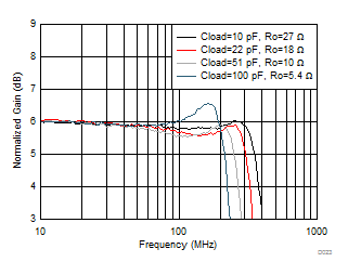
THS4541-Q1 D023_SLOS375.gif
100 mVPP at load, Av = 2 (see Figure 71), two series Ro added at output before Cload
Figure 23. Small-Signal Frequency Response vs Cload
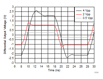
THS4541-Q1 D025_SLOS375.gif
50-MHz input, 0.3-ns input edge rate, single-ended input to differential output, DC coupled, see Figure 63
Figure 25. Small- and Large-Signal Step Response
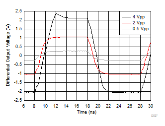
THS4541-Q1 D027_SLOS375.gif
G = 5 V/V, 50-MHz input, 0.3-ns input edge rate, single-ended input to differential output, see Figure 61
Figure 27. Small- and Large-Signal Step Response
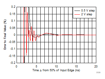
THS4541-Q1 D029_SLOS375.gif
Simulated with 2-ns input transition time, see Figure 63
Figure 29. Small- and Large-Signal Step Settling Time
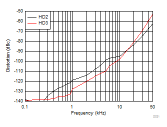
THS4541-Q1 D031_SLOS375.gif
2-VPP output, see Figure 61 with Vs+ = 3 V, Vocm = 1.5 V
Figure 31. Harmonic Distortion Over Frequency
THS4541-Q1 D033_SLOS375.gif
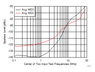
1 VPP each tone, see Figure 61 with Vs+ = 3 V, Vocm = 1.5 V
Figure 33. IMD2 and IM3 Over Frequency
THS4541-Q1 D035_SLOS375.gif
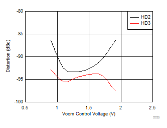
f = 10 MHz, 2-VPP output, see Figure 63 with Vocm adjusted
Figure 35. Harmonic Distortion vs Vocm
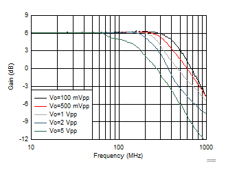
THS4541-Q1 D020_SLOS375.gif
See Figure 61 with VCC = 3 V and Vocm = 1.5 V
Figure 20. Frequency Response vs Vopp
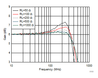
THS4541-Q1 D022_SLOS375.gif
Vout = 100 mVPP, see Figure 61 with the Rload adjusted
Figure 22. Small-Signal Frequency Response vs Rload
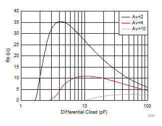
THS4541-Q1 D024_SLOS375.gif
Two Ro at output to differential Cload in parallel with 500 Ω, see Figure 71 and Table 6
Figure 24. Recommended Ro vs Cload
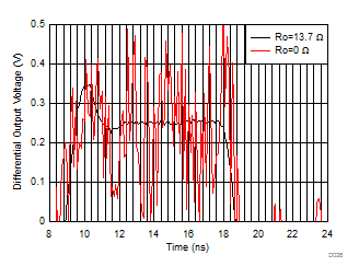
THS4541-Q1 D026_SLOS375.gif
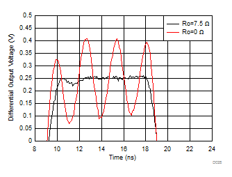
500-mVPP output into 22-pF Cload, see Figure 71 with Vs+ = 3 V and Vocm = 1.5 V
Figure 26. Step Response into Capacitive Load
THS4541-Q1 D028_SLOS375.gif
G = 5 V/V, 500-mVpp output into 22-pF Cload, see Figure 71 and Table 6
Figure 28. Step Response into Capacitive Load
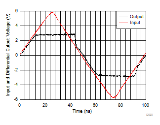
THS4541-Q1 D030_SLOS375.gif
Single-ended to differential gain of 2 (see Figure 63), > 2x input overdrive
Figure 30. Overdrive Recovery Performance
THS4541-Q1 D032_SLOS375.gif
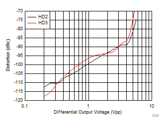
f = 10 MHz, see Figure 61 with Vs+ = 3 V, Vocm = 1.5 V
Figure 32. Harmonic Distortion vs Output Swing
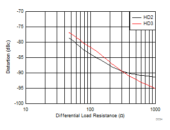
THS4541-Q1 D034_SLOS375.gif
f = 10 MHz, see Figure 61 with Vs+ = 3 V, Vocm = 1.5 V
Figure 34. Harmonic Distortion vs Rload
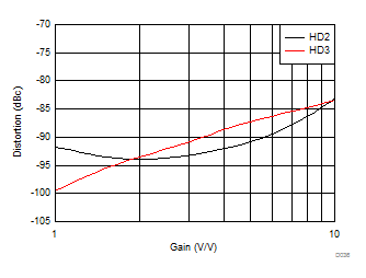
THS4541-Q1 D036_SLOS375.gif
f = 10 MHz, 2-VPP output, see Figure 61 and Table 6 for gain setting
Figure 36. Harmonic Distortion vs Gain