SLOS930B November 2015 – November 2019 THS4541-Q1
PRODUCTION DATA.
- 1 Features
- 2 Applications
- 3 Description
- 4 Revision History
- 5 Device Comparison Table
- 6 Pin Configuration and Functions
- 7 Specifications
-
8 Parameter Measurement Information
- 8.1 Example Characterization Circuits
- 8.2 Frequency-Response Shape Factors
- 8.3 I/O Headroom Considerations
- 8.4 Output DC Error and Drift Calculations and the Effect of Resistor Imbalances
- 8.5 Noise Analysis
- 8.6 Factors Influencing Harmonic Distortion
- 8.7 Driving Capacitive Loads
- 8.8 Thermal Analysis
-
9 Detailed Description
- 9.1 Overview
- 9.2 Functional Block Diagram
- 9.3 Feature Description
- 9.4
Device Functional Modes
- 9.4.1
Operation from Single-Ended Sources to Differential Outputs
- 9.4.1.1 AC-Coupled Signal Path Considerations for Single-Ended Input to Differential Output Conversion
- 9.4.1.2 DC-Coupled Input Signal Path Considerations for Single-Ended to Differential Conversion
- 9.4.1.3 Resistor Design Equations for the Single-Ended to Differential Configuration of the FDA
- 9.4.1.4 Input Impedance for the Single-Ended to Differential FDA Configuration
- 9.4.2 Differential-Input to Differential-Output Operation
- 9.4.1
Operation from Single-Ended Sources to Differential Outputs
- 10Application and Implementation
- 11Power Supply Recommendations
- 12Layout
- 13Device and Documentation Support
- 14Mechanical, Packaging, and Orderable Information
Package Options
Mechanical Data (Package|Pins)
- RGT|16
Thermal pad, mechanical data (Package|Pins)
- RGT|16
Orderable Information
7.7.3 3-V to 5-V Supply Range
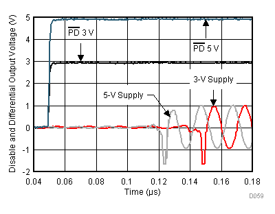
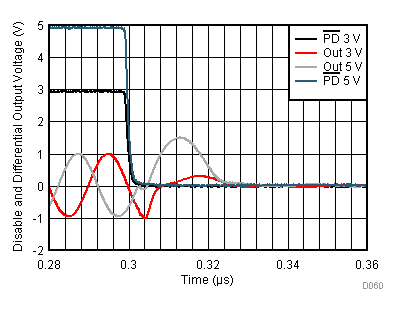
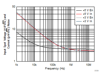
at Vs+ = 3 V and 5 V, Vs– = GND, Vocm is open, 50-Ω single-ended input to differential output, gain = 2 V/V, Rload = 500 Ω, and TA ≈ 25°C (unless otherwise noted)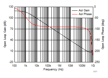
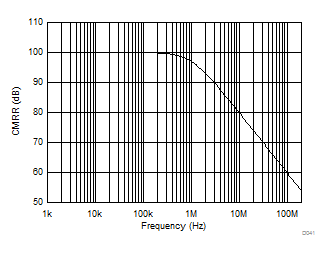
| Common-mode in to differential out, gain of 2 simulation | ||
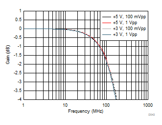 Figure 43. Common-Mode, Small- and Large-Signal Response (Vocm pin driven)
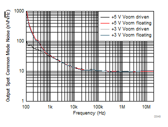
| Vocm input either driven to midsupply by low impedance source, or allowed to float and default to midsupply |
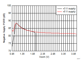
| Single-ended to differential gain of 2 (see Figure 61), PSRR for negative supply to differential output (1-kHz simulation) |
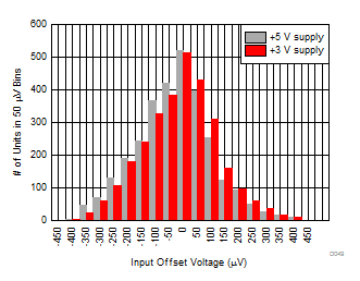
| 3 lots, total of 2962 units trimmed at 5-V supply |
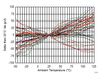
| 5-V and 3-V delta from 25°C VIO, 25 units |
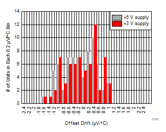
| –40°C to +125°C endpoint drift, 3 lots, total of 68 units |
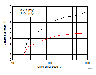
| Maximum differential output swing, Vocm at midsupply |
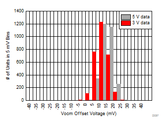
| Vocm input floating, 3 lots, total of 2962 units |
Default Value
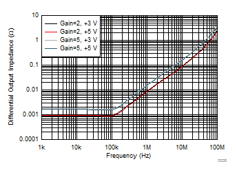
| Single-ended input to differential output, simulated differential output impedance, (closed-loop) gain of 2 and 5, see Figure 61 |
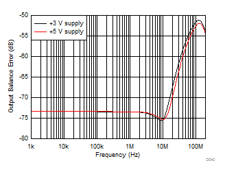
| Single-ended input to differential output, gain of 2 (see Figure 61), simulated with 1% resistor, worst-case mismatch |
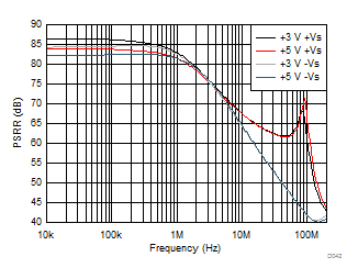
| Single-ended to differential, gain of 2 (see Figure 61) PSRR simulated to differential output |
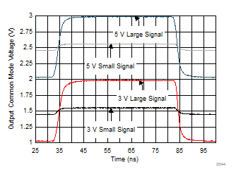 Figure 44. Common-Mode, Small- and Large-Step Response (Vocm pin driven)
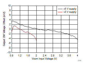
| Average Vocm output offset of 37 units,
Standard deviation < 2.5 mV, see Figure 63 |
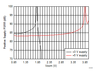
| Single-ended to differential gain of 2 (see Figure 61), PSRR for positive supply to differential output (1-kHz simulation) |
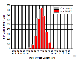
| 3 lots, total of 2962 units |
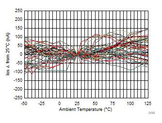
| 5-V and 3-V over temperature IOS, 25 units |
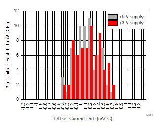
| –40°C to +125°C endpoint drift, 3 lots, total of 68 units |
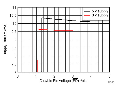
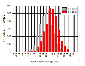
| Input driven midsupply, 3 lots, total of 2962 units |
