SLOS930B November 2015 – November 2019 THS4541-Q1
PRODUCTION DATA.
- 1 Features
- 2 Applications
- 3 Description
- 4 Revision History
- 5 Device Comparison Table
- 6 Pin Configuration and Functions
- 7 Specifications
-
8 Parameter Measurement Information
- 8.1 Example Characterization Circuits
- 8.2 Frequency-Response Shape Factors
- 8.3 I/O Headroom Considerations
- 8.4 Output DC Error and Drift Calculations and the Effect of Resistor Imbalances
- 8.5 Noise Analysis
- 8.6 Factors Influencing Harmonic Distortion
- 8.7 Driving Capacitive Loads
- 8.8 Thermal Analysis
-
9 Detailed Description
- 9.1 Overview
- 9.2 Functional Block Diagram
- 9.3 Feature Description
- 9.4
Device Functional Modes
- 9.4.1
Operation from Single-Ended Sources to Differential Outputs
- 9.4.1.1 AC-Coupled Signal Path Considerations for Single-Ended Input to Differential Output Conversion
- 9.4.1.2 DC-Coupled Input Signal Path Considerations for Single-Ended to Differential Conversion
- 9.4.1.3 Resistor Design Equations for the Single-Ended to Differential Configuration of the FDA
- 9.4.1.4 Input Impedance for the Single-Ended to Differential FDA Configuration
- 9.4.2 Differential-Input to Differential-Output Operation
- 9.4.1
Operation from Single-Ended Sources to Differential Outputs
- 10Application and Implementation
- 11Power Supply Recommendations
- 12Layout
- 13Device and Documentation Support
- 14Mechanical, Packaging, and Orderable Information
Package Options
Mechanical Data (Package|Pins)
- RGT|16
Thermal pad, mechanical data (Package|Pins)
- RGT|16
Orderable Information
8.7 Driving Capacitive Loads
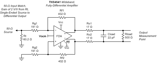
A very common requirement is driving the capacitive load of an ADC or some other next stage device. Directly driving a capacitive load with a closed-loop amplifier such as the THS4541-Q1 can lead to an unstable response, as shown in the step response plots into a capacitive load (see Figure 8 and Figure 26). One typical remedy for this instability is to add two small series resistors (Ro in Figure 71) at the outputs of the THS4541-Q1. Figure 6 and Figure 24 provide parametric plots of recommended Ro values versus differential capacitive load values and gain.
 Figure 71. Including Ro when Driving Capacitive Loads
 Operating at higher gains requires lower Ro values to achieve a ±0.5-dB flat response for the same capacitive load. Some direct parasitic loading is acceptable with no series Ro that increases with gain setting, as illustrated in Figure 6 and Figure 24 where the Ro value is 0 Ω. Even when these plots suggest no series Ro is required, good practice is to include a place for the Ro elements in the board layout (0-Ω load initially) for later adjustment, in case the response appears unacceptable. The TINA simulation model does a good job of predicting this effect and showing the impact for different choices of capacitive load isolating resistors (Ro).