JAJSFC6C May   2015  – April 2018 ADS52J90

PRODUCTION DATA.  

  1. 特長
  2. アプリケーション
  3. 概要
    1.     概略回路図
  4. 改訂履歴
  5. 概要(続き)
  6. Pin Configuration and Functions
    1.     Pin Functions
  7. Specifications
    1. 7.1  Absolute Maximum Ratings
    2. 7.2  ESD Ratings
    3. 7.3  Recommended Operating Conditions
    4. 7.4  Thermal Information
    5. 7.5  Electrical Characteristics
    6. 7.6  Digital Characteristics
    7. 7.7  Timing Requirements: Signal Chain
    8. 7.8  Timing Requirements: JESD Interface
    9. 7.9  Timing Requirements: Serial Interface
    10. 7.10 Typical Characteristics
    11. 7.11 Typical Characteristics: JESD Interface
    12. 7.12 Typical Characteristics: Contour Plots
  8. Detailed Description
    1. 8.1 Overview
    2. 8.2 Functional Block Diagrams
    3. 8.3 Feature Description
      1. 8.3.1  Connection of the External Inputs to the Input Pins
      2. 8.3.2  Input Multiplexer and Sampler
      3. 8.3.3  Analog-to-Digital Converter (ADC)
      4. 8.3.4  Device Synchronization Using TX_TRIG
      5. 8.3.5  Digital Processing
        1. 8.3.5.1 Digital Offset
          1. 8.3.5.1.1 Manual Offset Correction
          2. 8.3.5.1.2 Auto Offset Correction Mode (Offset Correction using a Built-In Offset Calculation Function)
          3. 8.3.5.1.3 Digital Averaging
          4. 8.3.5.1.4 Digital Gain
          5. 8.3.5.1.5 Digital HPF
      6. 8.3.6  Data Formatting
      7. 8.3.7  Serializer and LVDS Interface
      8. 8.3.8  LVDS Buffers
      9. 8.3.9  JESD204B Interface
        1. 8.3.9.1 Overview
        2. 8.3.9.2 Link Configuration
        3. 8.3.9.3 JESD Version and Subclass
        4. 8.3.9.4 Transport Layer
          1. 8.3.9.4.1 User Data Format
          2. 8.3.9.4.2 Transport Layer Test Patterns
        5. 8.3.9.5 Scrambler
        6. 8.3.9.6 Data Link Layer
          1. 8.3.9.6.1 Code Group Synchronization (CGS)
          2. 8.3.9.6.2 Initial Lane Alignment (ILA)
          3. 8.3.9.6.3 Lane and Frame Alignment Monitoring
          4. 8.3.9.6.4 Link Layer Test Modes
        7. 8.3.9.7 Deterministic Latency
          1. 8.3.9.7.1 Synchronization Using SYNC~ and SYSREF
          2. 8.3.9.7.2 Latency
          3. 8.3.9.7.3 Multiframe Size
        8. 8.3.9.8 JESD Physical Layer
          1. 8.3.9.8.1 CML Buffer
          2. 8.3.9.8.2 Jitter Considerations
      10. 8.3.10 Interfacing SYNC~ and SYSREF Between the FPGA and ADCs
      11. 8.3.11 Clock Input
      12. 8.3.12 Analog Input and Driving Circuit
        1. 8.3.12.1 Signal Input
    4. 8.4 Device Functional Modes
      1. 8.4.1 Input Modes
      2. 8.4.2 ADC Resolution Modes
      3. 8.4.3 LVDS and JESD Interface Modes
      4. 8.4.4 LVDS Serialization and Output Data Rate Modes
      5. 8.4.5 Power Modes
      6. 8.4.6 LVDS Test Pattern Mode
    5. 8.5 Programming
      1. 8.5.1 Serial Peripheral Interface (SPI) Operation
        1. 8.5.1.1 Serial Register Write Description
        2. 8.5.1.2 Register Readout
  9. Application and Implementation
    1. 9.1 Application Information
    2. 9.2 Typical Application
      1. 9.2.1 Design Requirements
      2. 9.2.2 Detailed Design Procedure
        1. 9.2.2.1 Designing with the 16-Input Mode
        2. 9.2.2.2 Designing with the 32-Input Mode
        3. 9.2.2.3 Designing with the 8-Input Mode
      3. 9.2.3 Application Curves
    3. 9.3 Do's and Don'ts
  10. 10Power Supply Recommendations
    1. 10.1 Power Sequencing and Initialization
  11. 11Layout
    1. 11.1 Power Supply, Grounding, and Bypassing
    2. 11.2 Layout Guidelines
    3. 11.3 Layout Example
  12. 12Register Map
    1. 12.1 ADC Registers
      1. 12.1.1 Description of Registers
        1. 12.1.1.1  Register 0h (address = 0h)
          1. Table 47. Register 0h Field Descriptions
        2. 12.1.1.2  Register 1h (address = 1h)
          1. Table 48. Register 1h Field Descriptions
        3. 12.1.1.3  Register 2h (address = 2h)
          1. Table 51. Register 2h Field Descriptions
        4. 12.1.1.4  Register 3h (address = 3h)
          1. Table 53. Register 3h Field Descriptions
        5. 12.1.1.5  Register 4h (address = 4h)
          1. Table 54. Register 4h Field Descriptions
        6. 12.1.1.6  Register 5h (address = 5h)
          1. Table 55. Register 5h Field Descriptions
        7. 12.1.1.7  Register 7h (address = 7h)
          1. Table 56. Register 7h Field Descriptions
        8. 12.1.1.8  Register 8h (address = 8h)
          1. Table 57. Register 8h Field Descriptions
        9. 12.1.1.9  Register Ah (address = Ah)
          1. Table 58. Register Ah Field Descriptions
        10. 12.1.1.10 Register Bh (address = Bh)
          1. Table 59. Register Bh Field Descriptions
        11. 12.1.1.11 Register Dh (address = Dh)
          1. Table 60. Register Dh Field Descriptions
        12. 12.1.1.12 Register Eh (address = Eh)
          1. Table 61. Register Eh Field Descriptions
        13. 12.1.1.13 Register Fh (address = Fh)
          1. Table 62. Register Fh Field Descriptions
        14. 12.1.1.14 Register 10h (address = 10h)
          1. Table 63. Register 10h Field Descriptions
        15. 12.1.1.15 Register 11h (address = 11h)
          1. Table 64. Register 11h Field Descriptions
        16. 12.1.1.16 Register 12h (address = 12h)
          1. Table 65. Register 12h Field Descriptions
        17. 12.1.1.17 Register 13h (address = 13h)
          1. Table 66. Register 13h Field Descriptions
        18. 12.1.1.18 Register 14h (address = 14h)
          1. Table 67. Register 14h Field Descriptions
        19. 12.1.1.19 Register 15h (address = 15h)
          1. Table 68. Register 15h Field Descriptions
        20. 12.1.1.20 Register 17h (address = 17h)
          1. Table 69. Register 17h Field Descriptions
        21. 12.1.1.21 Register 18h (address = 18h)
          1. Table 70. Register 18h Field Descriptions
        22. 12.1.1.22 Register 19h (address = 19h)
          1. Table 71. Register 19h Field Descriptions
        23. 12.1.1.23 Register 1Ah (address = 1Ah)
          1. Table 72. Register 1Ah Field Descriptions
        24. 12.1.1.24 Register 1Bh (address = 1Bh)
          1. Table 73. Register 1Bh Field Descriptions
        25. 12.1.1.25 Register 1Ch (address = 1Ch)
          1. Table 74. Register 1Ch Field Descriptions
        26. 12.1.1.26 Register 1Dh (address = 1Dh)
          1. Table 75. Register 1Dh Field Descriptions
        27. 12.1.1.27 Register 1Eh (address = 1Eh)
          1. Table 76. Register 1Eh Field Descriptions
        28. 12.1.1.28 Register 1Fh (address = 1Fh)
          1. Table 77. Register 1Fh Field Descriptions
        29. 12.1.1.29 Register 20h (address = 20h)
          1. Table 78. Register 20h Field Descriptions
        30. 12.1.1.30 Register 21h (offset = 21h)
          1. Table 79. Register 21h Field Descriptions
        31. 12.1.1.31 Register 23h (register = 23h)
          1. Table 80. Register 23h Field Descriptions
        32. 12.1.1.32 Register 24h (address = 24h)
          1. Table 81. Register 24h Field Descriptions
        33. 12.1.1.33 Register 25h (address = 25h)
          1. Table 82. Register 25h Field Descriptions
        34. 12.1.1.34 Register 26h (address = 26h)
          1. Table 83. Register 26h Field Descriptions
        35. 12.1.1.35 Register 27h (address = 27h)
          1. Table 84. Register 27h Field Descriptions
        36. 12.1.1.36 Register 28h (address = 28h)
          1. Table 85. Register 28h Field Descriptions
        37. 12.1.1.37 Register 29h (address = 29h)
          1. Table 86. Register 29h Field Descriptions
        38. 12.1.1.38 Register 2Ah (address = 2Ah)
          1. Table 87. Register 2Ah Field Descriptions
        39. 12.1.1.39 Register 2Bh (address = 2Bh)
          1. Table 88. Register 2Bh Field Descriptions
        40. 12.1.1.40 Register 2Ch (address = 2Ch)
          1. Table 89. Register 2Ch Field Descriptions
        41. 12.1.1.41 Register 2Dh (address = 2Dh)
          1. Table 90. Register 2Dh Field Descriptions
        42. 12.1.1.42 Register 2Fh (address = 2Fh)
          1. Table 91. Register 2Fh Field Descriptions
        43. 12.1.1.43 Register 30h (address = 30h)
          1. Table 92. Register 30h Field Descriptions
        44. 12.1.1.44 Register 31h (address = 31h)
          1. Table 93. Register 31h Field Descriptions
        45. 12.1.1.45 Register 32h (address = 32h)
          1. Table 94. Register 32h Field Descriptions
        46. 12.1.1.46 Register 33h (address = 33h)
          1. Table 95. Register 33h Field Descriptions
        47. 12.1.1.47 Register 34h (address = 34h)
          1. Table 96. Register 34h Field Descriptions
        48. 12.1.1.48 Register 35h (address = 35h)
          1. Table 97. Register 35h Field Descriptions
        49. 12.1.1.49 Register 36h (address = 36h)
          1. Table 98. Register 36h Field Descriptions
        50. 12.1.1.50 Register 37h (address = 37h)
          1. Table 99. Register 37h Field Descriptions
        51. 12.1.1.51 Register 38h (address = 38h)
          1. Table 100. Register 38h Field Descriptions
        52. 12.1.1.52 Register 39h (address = 39h)
          1. Table 101. Register 39h Field Descriptions
        53. 12.1.1.53 Register 3Bh (address = 3Bh)
          1. Table 102. Register 3Bh Field Descriptions
        54. 12.1.1.54 Register 3Ch (address = 3Ch)
          1. Table 103. Register 3Ch Field Descriptions
        55. 12.1.1.55 Register 43h (address = 43h)
          1. Table 104. Register 43h Field Descriptions
    2. 12.2 JESD Serial Interface Registers
      1. 12.2.1 Description of JESD Serial Interface Registers
        1. 12.2.1.1  Register 70 (address = 46h)
          1. Table 106. Register 70 Field Descriptions
        2. 12.2.1.2  Register 73 (address = 49h)
          1. Table 107. Register 73 Field Descriptions
        3. 12.2.1.3  Register 74 (address = 4Ah)
          1. Table 108. Register 74 Field Descriptions
        4. 12.2.1.4  Register 75 (address = 4Bh)
          1. Table 109. Register 75 Field Descriptions
        5. 12.2.1.5  Register 77 (address = 4Dh)
          1. Table 110. Register 77 Field Descriptions
        6. 12.2.1.6  Register 80 (address = 50h)
          1. Table 111. Register 80 Field Descriptions
        7. 12.2.1.7  Register 81 (address = 51h)
          1. Table 112. Register 81 Field Descriptions
        8. 12.2.1.8  Register 82 (address = 52h)
          1. Table 113. Register 82 Field Descriptions
        9. 12.2.1.9  Register 83 (address = 53h)
          1. Table 114. Register 83 Field Descriptions
        10. 12.2.1.10 Register 85 (address = 55h)
          1. Table 115. Register 85 Field Descriptions
        11. 12.2.1.11 Register 115 (address = 73h)
          1. Table 116. Register 115 Field Descriptions
        12. 12.2.1.12 Register 116 (address = 74h)
          1. Table 117. Register 116 Field Descriptions
        13. 12.2.1.13 Register 117 (address = 75h)
          1. Table 118. Register 117 Field Descriptions
        14. 12.2.1.14 Register 118 (address = 76h)
          1. Table 119. Register 118 Field Descriptions
        15. 12.2.1.15 Register 119 (address = 77h)
          1. Table 120. Register 119 Field Descriptions
        16. 12.2.1.16 Register 120 (address = 78h)
          1. Table 121. Register 120 Field Descriptions
        17. 12.2.1.17 Register 134 (address = 86h)
          1. Table 122. Register 134 Field Descriptions
        18. 12.2.1.18 Register 135 (address = 87h)
          1. Table 123. Register 135 Field Descriptions
        19. 12.2.1.19 Register 136 (address = 88h)
          1. Table 124. Register 136 Field Descriptions
        20. 12.2.1.20 Register 137 (address = 89h)
          1. Table 125. Register 137 Field Descriptions
        21. 12.2.1.21 Register 138 (address = 8Ah)
          1. Table 126. Register 138 Field Descriptions
  13. 13デバイスおよびドキュメントのサポート
    1. 13.1 ドキュメントのサポート
      1. 13.1.1 関連資料
    2. 13.2 コミュニティ・リソース
    3. 13.3 商標
    4. 13.4 静電気放電に関する注意事項
    5. 13.5 Glossary
  14. 14メカニカル、パッケージ、および注文情報

パッケージ・オプション

メカニカル・データ(パッケージ|ピン)
  • ZZE|198
サーマルパッド・メカニカル・データ
発注情報

Clock Input

The input clock to the device (referred to as the system clock) goes to an input buffer that automatically configures itself either to accept a single-ended clock or a differential clock. The equivalent load on the clock pins in the case of a differential clock input is shown in Figure 85. For the case of a single-ended clock input, the 5-kΩ resistor is disconnected from the input.
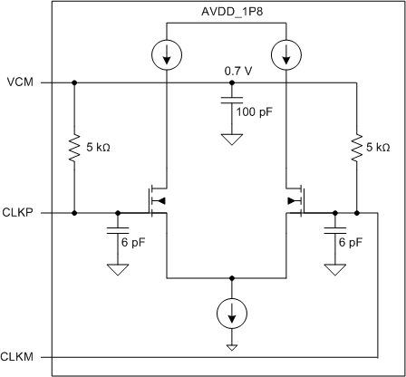
ADS52J90 Intrnl_Clck_Bffr.gifFigure 85. Internal Clock Buffer for Differential Clock Mode

If the preferred clocking scheme for the device is single-ended, connect the CLKM pin to ground (in other words, short CLKM directly to AVSS, as shown in Figure 86). In this case, the auto-detect feature shuts down the internal differential clock buffer and the device automatically goes into a single-ended clock input. Connect the single-ended clock source directly (without decoupling) to the CLKP pin. When using a single-ended clock input, TI recommends using low-jitter, square signals (LVCMOS levels, 1.8-V amplitude) to drive the ADC (refer to technical brief, Clocking High-Speed Data Converters, SLYT075 for further details).
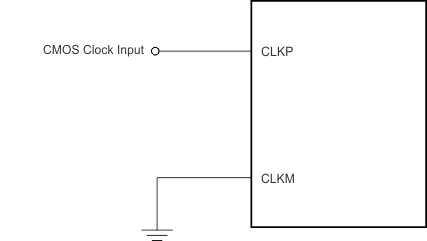
ADS52J90 ai_drv_cir_single_bas623.gifFigure 86. Single-Ended Clock Driving Circuit

For differential clocks (such as differential sine-wave, LVPECL, LVDS, and so forth), enable the clock amplifier with the connection scheme shown in Figure 87. This same scheme applies when the clock is single-ended but the clock amplitude is either small or its edges are not sharp. In this case, connect the input clock signal with a capacitor to CLKP (as in Figure 87) and connect CLKM to ground through a capacitor (that is, ac-coupled to AVSS).

If a transformer is used with the secondary coil floating (for instance, to convert from single-ended to differential), the outputs of the transformer can be connected directly to the clock inputs without requiring the 10-nF series capacitors.
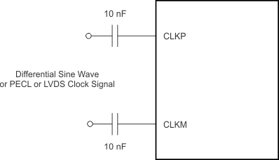
ADS52J90 ai_drv_cir_differential_bas623.gifFigure 87. Differential Clock Driving Circuit

To ensure that the aperture delay and jitter are the same for all channels, the device uses a clock tree network to generate individual sampling clocks for each channel. For all channels, the clock is closley matched from the source point to the sampling circuit of each of the eight internal devices.

The jitter cleaners CDCM7005, CDCE72010, or LMK048X series are suitable to generate the system clock and enable high performance. Figure 88 shows a clock distribution network.
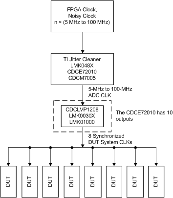
ADS52J90 ai_sys_clk_network_sbas623.gifFigure 88. System Clock Distribution Network