JAJSDY1C June 2017 – March 2018 TPS25740B
PRODUCTION DATA.
- 1 特長
- 2 アプリケーション
- 3 概要
- 4 改訂履歴
- 5 概要(続き)
- 6 Device Comparison Table
- 7 Pin Configuration and Functions
- 8 Specifications
-
9 Detailed Description
- 9.1 Overview
- 9.2 Functional Block Diagram
- 9.3
Feature Description
- 9.3.1 ENSRC
- 9.3.2 USB Type-C CC Logic (CC1, CC2)
- 9.3.3 USB PD BMC Transmission (CC1, CC2, VTX)
- 9.3.4 USB PD BMC Reception (CC1, CC2)
- 9.3.5 Discharging (DSCG, VPWR)
- 9.3.6 Configuring Voltage Capabilities (HIPWR)
- 9.3.7 Configuring Power Capabilities (PSEL, PCTRL, HIPWR)
- 9.3.8 Gate Driver (GDNG, GDNS)
- 9.3.9 Fault Monitoring and Protection
- 9.3.10 Voltage Control (CTL1, CTL2,CTL3)
- 9.3.11 Sink Attachment Indicator (DVDD)
- 9.3.12 Power Supplies (VAUX, VDD, VPWR, DVDD)
- 9.3.13 Grounds (AGND, GND)
- 9.3.14 Output Power Supply (DVDD)
- 9.4 Device Functional Modes
-
10Application and Implementation
- 10.1
Application Information
- 10.1.1 System-Level ESD Protection
- 10.1.2 Using ENSRC to Enable the Power Supply upon Sink Attachment
- 10.1.3 Use of GD Internal Clamp
- 10.1.4 Resistor Divider on GD for Programmable Start Up
- 10.1.5 Selection of the CTL1, CTL2, and CTL3 Resistors (R(FBL1), R(FBL2), and R(FBL3))
- 10.1.6 Voltage Transition Requirements
- 10.1.7 VBUS Slew Control using GDNG C(SLEW)
- 10.1.8 Tuning OCP using RF and CF
- 10.2 Typical Applications
- 10.3 System Examples
- 10.1
Application Information
- 11Power Supply Recommendations
- 12Layout
- 13デバイスおよびドキュメントのサポート
- 14メカニカル、パッケージ、および注文情報
パッケージ・オプション
メカニカル・データ(パッケージ|ピン)
- RGE|24
サーマルパッド・メカニカル・データ
- RGE|24
発注情報
9.3.9.2 Over-Current Protection (ISNS, VBUS)
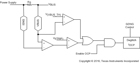
OCP protection is enabled tVP after the voltage on the VBUS pin has exceeded V(VBUS_RTH). Prior to OCP being enabled, the GD pin can be used to protect against a short.
The OCP protection circuit monitors the differential voltage across an external sense resistor to detect when the current outflow exceeds VI(TRIP) which in turn activates an over-current circuit breaker and disables the GDNG / GDNS gate driver. Once the OCP is enabled, if the voltage on the VBUS pin falls below V(VBUS_FTH) then that is also treated like an OCP event.
Following the recommended implementation of a 5-mΩ sense resistor, when the device is configured to deliver 3 A (via HIPWR pin), the OCP threshold lies between 3.8 A and 4.5 A. When configured to deliver 5 A (via HIPWR pin), the OCP threshold lies between 5.8 A and 6.8 A. The resistance of the sense resistor may be tuned to adjust the current that causes VI(TRIP) to be exceeded.
 Figure 35. Overcurrent Protection Circuit, (ISNS, VBUS)