JAJSDY1C June 2017 – March 2018 TPS25740B
PRODUCTION DATA.
- 1 特長
- 2 アプリケーション
- 3 概要
- 4 改訂履歴
- 5 概要(続き)
- 6 Device Comparison Table
- 7 Pin Configuration and Functions
- 8 Specifications
-
9 Detailed Description
- 9.1 Overview
- 9.2 Functional Block Diagram
- 9.3
Feature Description
- 9.3.1 ENSRC
- 9.3.2 USB Type-C CC Logic (CC1, CC2)
- 9.3.3 USB PD BMC Transmission (CC1, CC2, VTX)
- 9.3.4 USB PD BMC Reception (CC1, CC2)
- 9.3.5 Discharging (DSCG, VPWR)
- 9.3.6 Configuring Voltage Capabilities (HIPWR)
- 9.3.7 Configuring Power Capabilities (PSEL, PCTRL, HIPWR)
- 9.3.8 Gate Driver (GDNG, GDNS)
- 9.3.9 Fault Monitoring and Protection
- 9.3.10 Voltage Control (CTL1, CTL2,CTL3)
- 9.3.11 Sink Attachment Indicator (DVDD)
- 9.3.12 Power Supplies (VAUX, VDD, VPWR, DVDD)
- 9.3.13 Grounds (AGND, GND)
- 9.3.14 Output Power Supply (DVDD)
- 9.4 Device Functional Modes
-
10Application and Implementation
- 10.1
Application Information
- 10.1.1 System-Level ESD Protection
- 10.1.2 Using ENSRC to Enable the Power Supply upon Sink Attachment
- 10.1.3 Use of GD Internal Clamp
- 10.1.4 Resistor Divider on GD for Programmable Start Up
- 10.1.5 Selection of the CTL1, CTL2, and CTL3 Resistors (R(FBL1), R(FBL2), and R(FBL3))
- 10.1.6 Voltage Transition Requirements
- 10.1.7 VBUS Slew Control using GDNG C(SLEW)
- 10.1.8 Tuning OCP using RF and CF
- 10.2 Typical Applications
- 10.3 System Examples
- 10.1
Application Information
- 11Power Supply Recommendations
- 12Layout
- 13デバイスおよびドキュメントのサポート
- 14メカニカル、パッケージ、および注文情報
パッケージ・オプション
メカニカル・データ(パッケージ|ピン)
- RGE|24
サーマルパッド・メカニカル・データ
- RGE|24
発注情報
9.3.12 Power Supplies (VAUX, VDD, VPWR, DVDD)
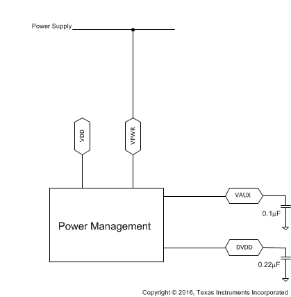
The VAUX pin is the output of a linear regulator and the input supply for internal power management circuitry. The VAUX regulator draws power from VDD after establishing a USB PD contract unless it is not available in which case it draws from VPWR. Changes in supply voltages will result in seamless switching between supplies.
If there is a load on the DVDD pin, that current will be drawn from the VPWR pin unless the device has stabilized into a USB PD contract or VPWR is below its UVLO.
Connect VAUX to GND via the recommended bypass capacitor. Do not connect any external load that draws more than I(VAUXEXT). Locate the bypass capacitor close to the pin and provide a low impedance ground connection from the capacitor to the ground plane.
VDD should either be grounded or be fed by a low impedance path and have input bypass capacitance. Locate the bypass capacitors close to the VDD and VPWR pins and provide a low impedance ground connection from the capacitor to the ground plane.
 Figure 37. Power Management