SPRAC94D September 2018 – March 2022 AFE030 , AFE031 , TMS320F28075 , TMS320F28075-Q1 , TMS320F28076 , TMS320F28374D , TMS320F28374S , TMS320F28375D , TMS320F28375S , TMS320F28375S-Q1 , TMS320F28376D , TMS320F28376S , TMS320F28377D , TMS320F28377D-EP , TMS320F28377D-Q1 , TMS320F28377S , TMS320F28377S-Q1 , TMS320F28379D , TMS320F28379D-Q1 , TMS320F28379S
- Trademarks
- 1 FSK Overview
- 2 Hardware Overview
- 3 Interfacing With the AFE03x
- 4 Transmit Path
- 5 Receive Path
- 6 Interfacing With a Power Line
- 7 Summary
- 8 References
- 9 Schematics
- 10Revision History
5.1 Receive Path Overview
The C2000 AFE031 system receive path is shown in Figure 5-1. There is a significant amount of filtering the input signal must traverse along the path from the transformer on the right to the input of the C2000 ADC on the left. On the AFE side, the AFE031 has vast filtering abilities for these signals.
 Figure 5-1 AFE031 Receive Path Interfaced
With C2000 ADC
Figure 5-1 AFE031 Receive Path Interfaced
With C2000 ADCThe AFE031 RX path consists of Rx PGA1, the Rx Low Pass Filter, and Rx PGA2. Both Rx PGA1 and Rx PGA2 are high performance programmable gain amplifiers that can be configured through SPI. Rx PGA1 can operate as either an attenuator, providing loss, or an amplifier, providing gain. The gain steps of the Rx PGA1 are 0.25 V/V, 0.5 V/V, 1 V/V, and 2 V/V. The gain steps of the Rx PGA2 are 1 V/V, 4 V/V, 16 V/V, and 64 V/V. For specific RX PGA Gain Select Register values, see Table 5-1. Configuring the Rx PGA1 as an attenuator (at gains less than 1 V/V) is useful for applications where the presence of large interference signals are present within the signal band. Attenuating the large interference allows these signals to pass through the analog Rx signal chain without causing an overload; the interference signal can then be processed and removed within the microcontroller, as necessary.
| Bit Name | Location (0 = LSB) | Default | R/W | Function |
|---|---|---|---|---|
| RX1G-0, RX1G-1 | 0,1 | 0,1 | R/W | This bit is used to set
the gain of the RX PGA1. 00 = 0.25 V/V 01 = 0.5 V/V 10 = 1 V/V 11 = 2 V/V |
| RX2G-0, RX2G-1 | 2,3 | 0,0 | R/W | This bit is used to set
the gain of the RX PGA2. 00 = 1 V/V 01 = 4 V/V 10 = 16 V/V 11 = 64 V/V |
The Rx filter is a very low noise, unity-gain, fourth-order low-pass filter. The Rx filter cutoff frequency is selectable between CENELEC A or CENELEC B,C,D modes that is set within the control register. Because the Rx filter is a very low noise analog filter, two external capacitors, shown in Figure 5-2, are required to properly configure the Rx filter. Table 5-2 shows the proper capacitance values for CENELEC A and B,C,D bands.
 Figure 5-2 External Filtering for the
AFE031 Receive Path
Figure 5-2 External Filtering for the
AFE031 Receive Path| Frequency Band | Rx C1, PIN 24 | Rx C2, PIN 23 | Cutoff Frequency (kHz) |
|---|---|---|---|
| CENELEC A | 680 pF | 680 pF | 90 |
| CENELEC B,C,D | 270 pF | 560 pF | 145 |
Capacitor Rx C1 is connected between pin 24 and ground, and Rx C2 is connected between pin 23 and ground. For the capacitors shown, it is recommended that these components be rated to withstand the full AVDD power-supply voltage.
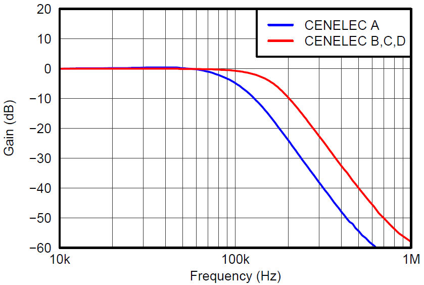
 Figure 5-3 RX Filter Gain vs.
Frequency
Figure 5-3 RX Filter Gain vs.
FrequencyThe gains witnessed at certain frequencies at the output of the RX low-pass filter are shown in Figure 5-3. This response displayed is under normal AFE03x operating conditions. Attenuation will begin at frequencies slightly before the actual cutoff frequencies in Table 5-2.
An external fourth-order passive passband filter is optional, but recommended for applications where high performance is required. The external passive passband filter removes any unwanted, out-of-band signals from the signal path, and prevents them from reaching the active internal filters within the AFE031. Table 5-3 shows the values needed for CENELEC A or CENELEC B,C,D with a 0dB passband. The component values used on the BoosterPack were for a CENELEC B,C,D with a 0dB passband.
| Frequency Band | Frequency Range (kHz) | Characteristic Impedance (Ω) | R1 (Ω) | R2 (Ω) | C1 (nF) | C2 (nF) | L1 (µH) | L2 (µH) |
|---|---|---|---|---|---|---|---|---|
| CENELEC A | 35 to 95 | 1k | 1k | 10k | 4.7 | 1.5 | 1500 | 4700 |
| CENELEC B,C,D | 95 to 150 | 1k | 1k | 10k | 1.7 | 1 | 1200 | 1500 |
| SFSK | 63 to 74 | 1k | 1 | 10k | 2.7 | 2.2 | 2200 | 2200 |
For other bandpass filter component values with a different passband attenuation, see the AFE031 Powerline Communications Analog Front-End Data Sheet .