SPRAC94D September   2018  – March 2022 AFE030 , AFE031 , TMS320F28075 , TMS320F28075-Q1 , TMS320F28076 , TMS320F28374D , TMS320F28374S , TMS320F28375D , TMS320F28375S , TMS320F28375S-Q1 , TMS320F28376D , TMS320F28376S , TMS320F28377D , TMS320F28377D-EP , TMS320F28377D-Q1 , TMS320F28377S , TMS320F28377S-Q1 , TMS320F28379D , TMS320F28379D-Q1 , TMS320F28379S


  1.   Trademarks
  2. FSK Overview
  3. Hardware Overview
    1. 2.1 Block Diagram
    2. 2.2 Hardware Setup
  4. Interfacing With the AFE03x
    1. 3.1 Configuring the AFE031
  5. Transmit Path
    1. 4.1 FSK Example Specifications
    2. 4.2 PWM Mode
      1. 4.2.1 Software Implementation
      2. 4.2.2 Testing Results
      3. 4.2.3 HRPWM vs. EPWM
    3. 4.3 DAC Mode
      1. 4.3.1 Software Implementation
      2. 4.3.2 Testing Results
      3. 4.3.3 OFDM Ability
    4. 4.4 Porting TX to LAUNCHXL-F280049C
      1. 4.4.1 PWM Mode Specific Porting
      2. 4.4.2 DAC Mode Specific Porting
  6. Receive Path
    1. 5.1 Receive Path Overview
    2. 5.2 Receiver Software Implementation
      1. 5.2.1 Initial Setup and Parameters
      2. 5.2.2 Interrupt Service Routines
      3. 5.2.3 Run Time Operation
      4. 5.2.4 Testing Results
      5. 5.2.5 System Utilization
      6. 5.2.6 Device Dependency and Porting
    3. 5.3 Tuning and Calibration
      1. 5.3.1 Setting the AFE03X's PGAs
      2. 5.3.2 Automatic Gain Control (AGC)
      3. 5.3.3 Setting the Bit Detection Threshold
      4. 5.3.4 FSK Correlation Detector Library
    4. 5.4 Porting RX to LAUNCHXL-F280049C
  7. Interfacing With a Power Line
    1. 6.1 Line Coupling
    2. 6.2 Coupling to an AC Line
      1. 6.2.1 Low Voltage Capacitor
      2. 6.2.2 The Ratio of the Transformer
      3. 6.2.3 HV Capacitor
      4. 6.2.4 HV Side Inductor
    3. 6.3 Coupling to DC Line
    4. 6.4 Protection Circuit
      1. 6.4.1 Metal Oxide Varistors
      2. 6.4.2 Transient Voltage Suppressors
      3. 6.4.3 Current Steering Diodes
    5. 6.5 Determining PA Power Supply Requirements
  8. Summary
  9. References
  10. Schematics
    1. 9.1 Schematics (PWM Mode)
    2. 9.2 Schematics (DAC Mode)
  11. 10Revision History

HV Capacitor

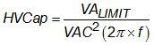
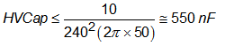
The high-voltage (HV) capacitor blocks the low-frequency mains voltage by forming a voltage divider with the winding inductance of the line coupling transformer. While using high voltage CBB capacitors, the maximum voltage range must exceed the amplitude of the power grid ac voltage. Operating the capacitor at approximately 80% of its ac-rated voltage ensures a long component operating life. The next important requirement is a standard setting maximum reactive power (VA limit). For example, the European product standards for attaching a device to the power grid must have a reactive power of less than 10 VAR, resulting in a capacitor values less than .55 µF. The equation below shows how the value .55 µF was used to determine the HV capacitor value.

Equation 3. GUID-6FD04588-9F32-4D37-B662-CC631C0031D7-low.gif

For a 240-VAC, 50-Hz application with a 10-VA limit,

Equation 4. GUID-385F2CF3-B09F-44AC-9943-469CE2ECCA18-low.gif

It is important to note that a metallized polypropylene electromagnetic interference and radio frequency interference (EMI/RFI) suppression capacitor is recommended because of the low loss factor associated with the dielectric, which results in minimal internal self-heating.