SPRAC94D September 2018 – March 2022 AFE030 , AFE031 , TMS320F28075 , TMS320F28075-Q1 , TMS320F28076 , TMS320F28374D , TMS320F28374S , TMS320F28375D , TMS320F28375S , TMS320F28375S-Q1 , TMS320F28376D , TMS320F28376S , TMS320F28377D , TMS320F28377D-EP , TMS320F28377D-Q1 , TMS320F28377S , TMS320F28377S-Q1 , TMS320F28379D , TMS320F28379D-Q1 , TMS320F28379S
- Trademarks
- 1 FSK Overview
- 2 Hardware Overview
- 3 Interfacing With the AFE03x
- 4 Transmit Path
- 5 Receive Path
- 6 Interfacing With a Power Line
- 7 Summary
- 8 References
- 9 Schematics
- 10Revision History
2.2 Hardware Setup
There are a few things that need to be done so that the hardware can be debugged correctly. Power is supplied to the BOOSTXL-AFE031 test board via the 15 V jumper. The BoosterPack has a regulator that will supply power to the LaunchPad connected. Figure 2-4 shows a close up of the 15 V headers.
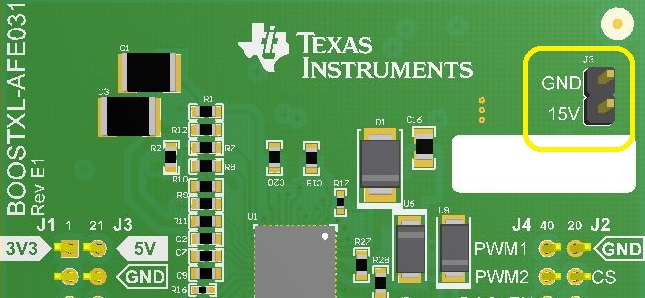 Figure 2-4 BOOSTXL-AFE031 Power Pins
The wire connected to the right input of the terminal block shown in Figure 2-5 will be the line that the transmitted output or received input FSK signal resides on, depending on whether the system is set up as a transmitter or receiver. The wire connected to the left input of the terminal block is the ground line. These lines can then be connected to some coupling circuitry or directly to another BOOSTXL-AFE031 terminal block for controlled testing, TX/RX to TX/RX and GND to GND.
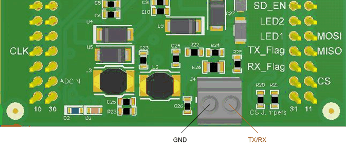 Figure 2-5 BOOSTXL-AFE031 Terminal Block Connections
Since the BoosterPack is supplying power to the launchPad, the PC USB interface needs to be isolated. Header jumpers JP1, JP2, and JP3 on the launchpad need to be removed to enable electrical isolation. Figure 2-6 is a close up of the location of the headers.
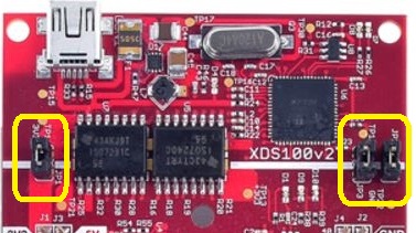 Figure 2-6 F28379D Jumper Configuration
When using the system as a FSK receiver, the LaunchPad needs 5 V to power the C2000 ADC. With the LaunchPad being isolated from the PC USB interface, the 5 V power rail needs to be generated by stepping up the supplied 3.3 V. Header JP6 on the LaunchPad needs to be added to enable the step-up regulator. Figure 2-7 is a close up of the location of the header.
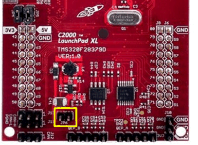 Figure 2-7 F28379D JP6 Location
When using the system as a receiver, make sure that the F28379D LaunchPad is version 2.0 or greater. Earlier versions (Ver 1.1 and 1.2) have an issue with the ADCIN pin that is connected to the BOOSTXL-AFE031. For more information, see the LAUNCHXL-F28379D Overview revisions section.
When using the transmitter solution in conjunction with the receiver solution, the complete system connection should look similar to what is shown in Figure 2-8.
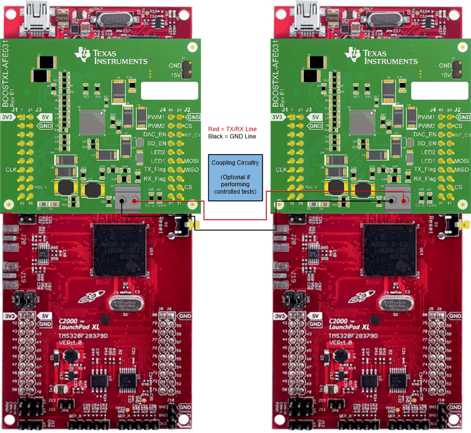 Figure 2-8 TX-RX Solution System