SPRAC94D September 2018 – March 2022 AFE030 , AFE031 , TMS320F28075 , TMS320F28075-Q1 , TMS320F28076 , TMS320F28374D , TMS320F28374S , TMS320F28375D , TMS320F28375S , TMS320F28375S-Q1 , TMS320F28376D , TMS320F28376S , TMS320F28377D , TMS320F28377D-EP , TMS320F28377D-Q1 , TMS320F28377S , TMS320F28377S-Q1 , TMS320F28379D , TMS320F28379D-Q1 , TMS320F28379S
- Trademarks
- 1 FSK Overview
- 2 Hardware Overview
- 3 Interfacing With the AFE03x
- 4 Transmit Path
- 5 Receive Path
- 6 Interfacing With a Power Line
- 7 Summary
- 8 References
- 9 Schematics
- 10Revision History
4.3.3 OFDM Ability
Although not implemented, the ability to do OFDM Frequency modulation is possible using the DAC mode of the AFE device. Being able to select the exact DAC value at every point gives the ability to combine frequency components on the MCU side, and set the DAC to the desired value.
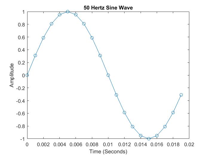
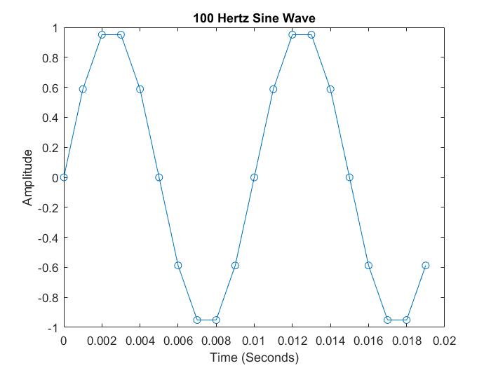
An example of combining two frequencies is shown in Figure 4-12 through Figure 4-15, which showcases how this can be accomplished. The two signals are 50 Hz and 100 Hz sine wave. To send these out independently, each point is discretely sent at the correct time interval to create the sine wave.
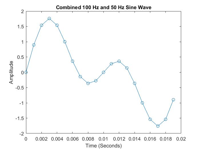
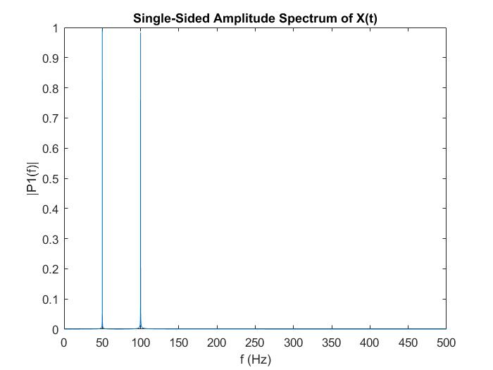
To send both frequencies out at the same time, the frequencies would need to be combined first. The result is shown in Figure 4-14. To send out each point in this waveform, the system would be sending two frequencies out at once. An FFT is performed on the data to see the two discrete frequencies.
 Figure 4-12 60 Hz Sine Wave
 Figure 4-14 60 + 100 Hz Sine Wave
 Figure 4-13 100 Hz Sine Wave
 Figure 4-15 FFT of Combined Signals