SPRAC94D September 2018 – March 2022 AFE030 , AFE031 , TMS320F28075 , TMS320F28075-Q1 , TMS320F28076 , TMS320F28374D , TMS320F28374S , TMS320F28375D , TMS320F28375S , TMS320F28375S-Q1 , TMS320F28376D , TMS320F28376S , TMS320F28377D , TMS320F28377D-EP , TMS320F28377D-Q1 , TMS320F28377S , TMS320F28377S-Q1 , TMS320F28379D , TMS320F28379D-Q1 , TMS320F28379S
- Trademarks
- 1 FSK Overview
- 2 Hardware Overview
- 3 Interfacing With the AFE03x
- 4 Transmit Path
- 5 Receive Path
- 6 Interfacing With a Power Line
- 7 Summary
- 8 References
- 9 Schematics
- 10Revision History
4.3 DAC Mode
This section describes one way to create a DAC mode FSK transmitter. DAC Mode is very similar to the PWM Mode, in that PWM interrupts are used to accomplish FSK transmission.
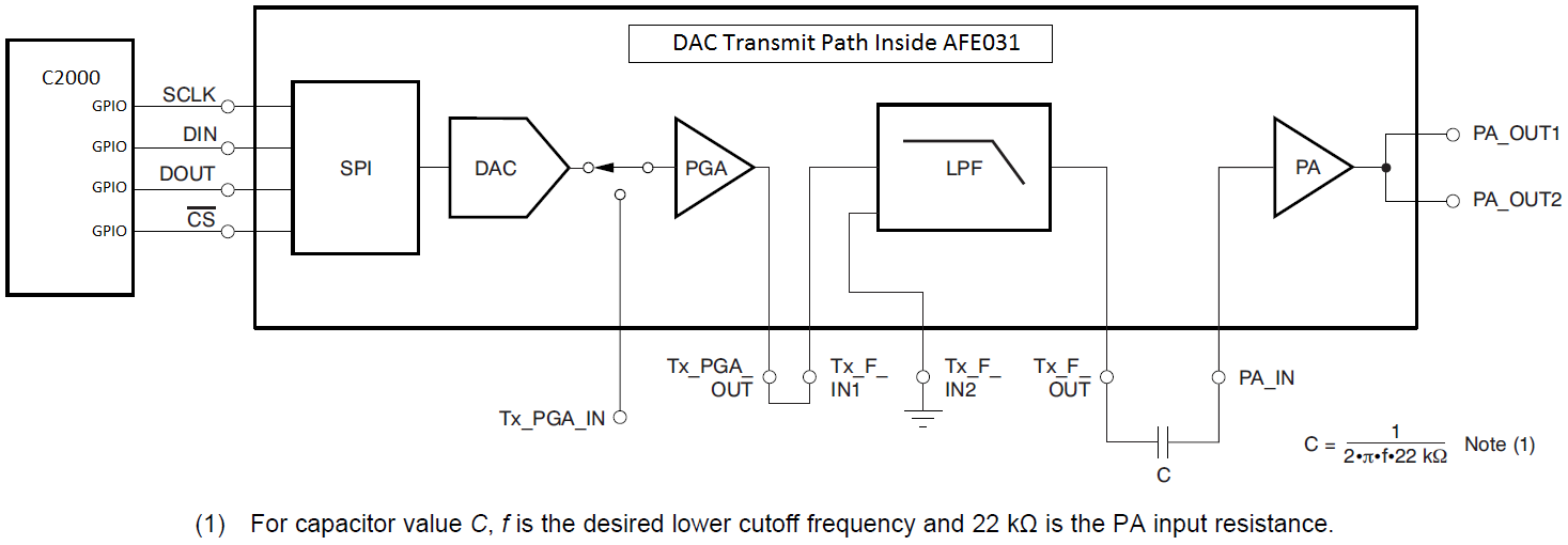
The transmit path utilized when using DAC mode is shown in Figure 4-7.
 Figure 4-7 DAC Transmit Path
In DAC mode, the software sends data over SPI to the internal DAC to set the output value. To accomplish sending a single tone, or sine wave, a ramp of DAC values at a given frequency are sent. Using a PWM interrupt occurring every period, send the updated DAC value at a frequency determined by the PWM period. The number of points in the sine table and desired frequency will determine the frequency of the PWM signal. For example, if given a 100 kHz sine wave that has ten points, all ten points need to be sent within 100 kHz. This means that the PWM has to generate an interrupt that follows the following formula:
PWM Frequency = Points of Sine Table * Desired Frequency
Figure 4-8 shows what this looks like in the time domain.
 Figure 4-8 DAC Sine Wave Ramp