TIDUCL0 January   2017


  1. Description
  2. Resources
  3. Features
  4. Applications
  5. Design Images
  6. System Overview
    1. 6.1 System Description
    2. 6.2 Key System Specifications
    3. 6.3 Block Diagram
    4. 6.4 Highlighted Products
      1. 6.4.1 CSD88584Q5DC
      2. 6.4.2 DRV8323
      3. 6.4.3 MSP430F5132
      4. 6.4.4 TPS54061
      5. 6.4.5 LMT87
  7. System Design Theory
    1. 7.1 Power Stage Design—Battery Power Input to the Board
    2. 7.2 Power Stage Design—Three-Phase Inverter
      1. 7.2.1 Design Considerations in Paralleling MOSFETs
        1. 7.2.1.1 Conduction Phase
        2. 7.2.1.2 Switching Phase
      2. 7.2.2 Selecting the Sense Resistor
    3. 7.3 Power Stage Design—DRV8323 Gate Driver
      1. 7.3.1 Gate Drive Features of DRV8323
      2. 7.3.2 Current Shunt Amplifier in DRV8323
      3. 7.3.3 Protection Features in DRV8323
    4. 7.4 Power Stage Design—18-V to 3.3-V DC-DC Converter
    5. 7.5 Power Stage Design —Microcontroller MSP430
    6. 7.6 Power Stage Design—Hall Sensor Interface
    7. 7.7 Temperature Sensing
    8. 7.8 Power Stage Design—External Interface Options and Indications
      1. 7.8.1 Speed Control of Motor
      2. 7.8.2 Direction of Rotation—Digital Input
      3. 7.8.3 LED Indications
      4. 7.8.4 Signal Interface Connector for External Monitoring and Control
  8. Getting Started Hardware and Software
    1. 8.1 Hardware
      1. 8.1.1 Connector Configuration of TIDA-00774
      2. 8.1.2 Programming of MSP430
      3. 8.1.3 Procedure for Board Bring-up and Testing
    2. 8.2 Software
      1. 8.2.1 System Features
      2. 8.2.2 Customizing the Reference Code
        1. 8.2.2.1 PWM_PERIOD
        2. 8.2.2.2 MAX_DUTYCYCLE
        3. 8.2.2.3 MIN_DUTYCYCLE
        4. 8.2.2.4 ACCEL_RATE
        5. 8.2.2.5 Block_Rotor_Duration
      3. 8.2.3 Configuring the DRV8323 Registers (drv8323.c)
      4. 8.2.4 Initializing SPI Communication Between DRV8323 and MSP430 (drv8323.h)
      5. 8.2.5 Running Project in Code Composer Studio (CCS)
  9. Testing and Results
    1. 9.1 Test Setup
    2. 9.2 Test Data
      1. 9.2.1 Functional Tests
        1. 9.2.1.1 3.3-V Power Supply Generated by Step-Down Converter
        2. 9.2.1.2 Gate Drive Voltage Generated by Gate Driver
        3. 9.2.1.3 Dead Time From DRV8323
        4. 9.2.1.4 MOSFET Switching Waveforms
        5. 9.2.1.5 VGS Skew of Parallel FETs During Switching
      2. 9.2.2 Load Test
        1. 9.2.2.1 Load Test Without Heat Sink
        2. 9.2.2.2 Load Test With Heat Sink
        3. 9.2.2.3 Load Test With Heat Sink and Airflow
      3. 9.2.3 Inverter Efficiency Test
      4. 9.2.4 Thermal Rise at Different Power Levels
      5. 9.2.5 Inverter Current Sensing by VDS Monitoring
      6. 9.2.6 Overcurrent and Short-Circuit Protection Test
        1. 9.2.6.1 Cycle-by-Cycle Stall Current Protection by DRV8323 VDS Sensing
        2. 9.2.6.2 Stall Current Latch Protection by DRV8323 VDS Sensing
      7. 9.2.7 Testing for Peak Current Capability
  10. 10Design Files
    1. 10.1 Schematics
    2. 10.2 Bill of Materials
    3. 10.3 PCB Layout Recommendations
      1. 10.3.1 Layout Prints
    4. 10.4 Altium Project
    5. 10.5 Gerber Files
    6. 10.6 Assembly Drawings
  11. 11Software Files
  12. 12Related Documentation
    1. 12.1 Trademarks
  13. 13Terminology
  14. 14About the Author

Power Stage Design—Battery Power Input to the Board

The battery power input section is shown in Figure 2. The input bulk aluminum electrolytic capacitors C14, C15, and C16 provide the ripple current and its voltage rating is de-rated by 50% for better life. These capacitors are rated to carry high ripple current. C17 is used as bypass capacitors to GND. D1 is the transient voltage suppression (TVS) having breakdown voltage of 30 V and maximum supply voltage of 30 V.
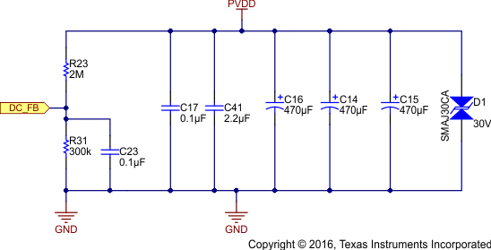
TIDA-00774 tida-00774-schematic-battery-power-input.gifFigure 2. Schematic of Battery Power Input Section

The input supply voltage PVDD is scaled using the resistive divider network, which consists of R23, R31, and C23, and fed to the MCU. Considering the maximum voltage for the MCU ADC input as 3.3 V, the maximum DC input voltage measurable by the MCU is calculated as in Equation 1.

Equation 1. TIDA-00774 tida-00774-equation-01.gif

Considering a 20% headroom for this value, the maximum recommended voltage input to the system is 25.3 × 0.8 = 20.25. So for a power stage with maximum operating voltage of 21 V, this voltage feedback resistor divider is ideal. Also, this choice gives optimal ADC resolution for a system operating from
6 to 21 V.