SNLA437 December 2023 DP83822H , DP83822HF , DP83822I , DP83822IF , DP83825I , DP83826E , DP83826I
- 1
- Abstract
- Trademarks
- 1DP83822 Application Overview
-
2Troubleshooting the PHY Application
- 2.1 Schematic and Layout Checklist
- 2.2 Verify Successful Power-up of PHY
- 2.3 Read and Check Register Values
- 2.4 Peripheral Pin Checks
- 2.5 Verifying Strap Configurations During Initialization
- 2.6 Debugging Link Quality
- 2.7 Built-In Self Test With Various Loopback Modes
- 2.8 Debug the Fiber Connection
- 2.9 Debug the MAC Interface
- 2.10 Debug the Start of Frame Detect
- 2.11 Tools and References
- 3References
2.5 Verifying Strap Configurations During Initialization
The strap values can be read from registers 0x467 (SOR_1) and 0x468 (SOR2), these registers are extended registers and can only be accessed using Extended Register Access. In the cases that the read strap value differs from the desired strap configurations, the voltage levels of the strap pins can be measured. Measurements can be made during power up and after power up when the RESET_N signal is asserted. Strap configurations can also be verified with the strap tool built in the DP83822 Schematic Checklist.
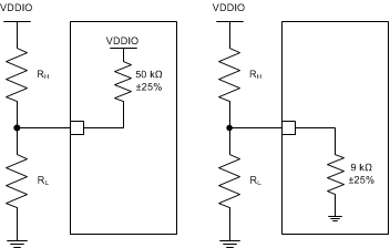
The DP83822 uses the receive path functional pins as bootstrap options to place the device into specific modes of operation. The values of these pins are sampled at power up or hardware reset, through either the RESET pin or bit[15] in the PHY Reset Control Register (PHYRCR, address 0x001F). The DP83822 bootstrap pins are 4-level, which are described in greater detail below. Because bootstrap pins may have alternate functions after reset is de-asserted, they should not be connected directly to VCC or GND. Pullup and pulldown resistors are required for proper operation.
Configuration of the device may be done via 4-level strapping or via serial management interface. A pullup resistor and a pulldown resistor of suggested values should be used to set the voltage ratio of the bootstrap pin input and the supply to select one of the possible modes.
 Figure 2-7 Bootstrap Circuits
| Mode (1) | Ideal RH (kΩ) | Ideal RL (kΩ) |
|---|---|---|
| PULLDOWN PINS (9 kΩ) | ||
| 1 (Default) | OPEN | OPEN |
| 2 | 10 | 2.49 |
| 3 | 5.76 | 2.49 |
| 4 | 2.49 | OPEN |
| PULLUP PINS (50 kΩ) | ||
| 1 | OPEN | 1.96 |
| 2 | 13 | 1.96 |
| 3 | 6.2 | 1.96 |
| 4 (Default) | OPEN | OPEN |
| Target Voltage (1) | Mode 1 | Mode 2 | Mode 3 | Mode 4 |
|---|---|---|---|---|
| Vmax (V) | 0.098 x VDDIO | 0.181 x VDDIO | 0.277 x VDDIO | VDDIO |
| Vtyp (V) | 0 | 0.165 x VDDIO | 0.252 x VDDIO | VDDIO |
| Vmin (V) | 0 | 0.148 x VDDIO | 0.227 x VDDIO | 0.694 x VDDIO |