TIDUE53I march   2018  – july 2023 TMS320F28P550SJ , TMS320F28P559SJ-Q1


  1.   1
  2.   Description
  3.   Resources
  4.   Features
  5.   Applications
  6.   6
  7. 1System Description
    1. 1.1 Key System Specifications
  8. 2System Overview
    1. 2.1 Block Diagram
    2. 2.2 Highlighted Products
      1. 2.2.1  UCC21710
      2. 2.2.2  UCC5320
      3. 2.2.3  TMS320F28379D
      4. 2.2.4  AMC1305M05
      5. 2.2.5  OPA4340
      6. 2.2.6  LM76003
      7. 2.2.7  PTH08080W
      8. 2.2.8  TLV1117
      9. 2.2.9  OPA350
      10. 2.2.10 UCC14240
    3. 2.3 System Design Theory
      1. 2.3.1 Three-Phase T-Type Inverter
        1. 2.3.1.1 Architecture Overview
        2. 2.3.1.2 LCL Filter Design
        3. 2.3.1.3 Inductor Design
        4. 2.3.1.4 SiC MOSFETs Selection
        5. 2.3.1.5 Loss Estimations
        6. 2.3.1.6 Thermal Considerations
      2. 2.3.2 Voltage Sensing
      3. 2.3.3 Current Sensing
      4. 2.3.4 System Power Supplies
        1. 2.3.4.1 Main Input Power Conditioning
        2. 2.3.4.2 Isolated Bias Supplies
      5. 2.3.5 Gate Drivers
        1. 2.3.5.1 1200-V SiC MOSFETs
        2. 2.3.5.2 650-V SiC MOSFETs
        3. 2.3.5.3 Gate Driver Bias Supply
      6. 2.3.6 Control Design
        1. 2.3.6.1 Current Loop Design
        2. 2.3.6.2 PFC DC Bus Voltage Regulation Loop Design
  9. 3Hardware, Software, Testing Requirements, and Test Results
    1. 3.1 Required Hardware and Software
      1. 3.1.1 Hardware
        1. 3.1.1.1 Test Hardware Required
        2. 3.1.1.2 Microcontroller Resources Used on the Design (TMS320F28379D)
        3. 3.1.1.3 F28377D, F28379D Control-Card Settings
        4. 3.1.1.4 Microcontroller Resources Used on the Design (TMS320F280039C)
      2. 3.1.2 Software
        1. 3.1.2.1 Getting Started With Firmware
          1. 3.1.2.1.1 Opening the CCS project
          2. 3.1.2.1.2 Digital Power SDK Software Architecture
          3. 3.1.2.1.3 Interrupts and Lab Structure
          4. 3.1.2.1.4 Building, Loading and Debugging the Firmware
        2. 3.1.2.2 Protection Scheme
        3. 3.1.2.3 PWM Switching Scheme
        4. 3.1.2.4 ADC Loading
    2. 3.2 Testing and Results
      1. 3.2.1 Lab 1
      2. 3.2.2 Testing Inverter Operation
        1. 3.2.2.1 Lab 2
        2. 3.2.2.2 Lab 3
        3. 3.2.2.3 Lab 4
      3. 3.2.3 Testing PFC Operation
        1. 3.2.3.1 Lab 5
        2. 3.2.3.2 Lab 6
        3. 3.2.3.3 Lab 7
      4. 3.2.4 Test Setup for Efficiency
      5. 3.2.5 Test Results
        1. 3.2.5.1 PFC Mode - 230 VRMS, 400 V L-L
          1. 3.2.5.1.1 PFC Start-up – 230 VRMS, 400 L-L AC Voltage
          2. 3.2.5.1.2 Steady State Results at 230 VRMS, 400 V L-L - PFC Mode
          3. 3.2.5.1.3 Efficiency and THD Results at 220 VRMS, 50 Hz – PFC Mode
          4. 3.2.5.1.4 Transient Test With Step Load Change
        2. 3.2.5.2 PFC Mode - 120 VRMS, 208 V L-L
          1. 3.2.5.2.1 Steady State Results at 120 VRMS, 208 V-L-L - PFC Mode
          2. 3.2.5.2.2 Efficiency and THD Results at 120 VRMS - PFC Mode
        3. 3.2.5.3 Inverter Mode
          1. 3.2.5.3.1 Inverter Closed Loop Results
          2. 3.2.5.3.2 Efficiency and THD Results - Inverter Mode
          3. 3.2.5.3.3 Inverter - Transient Test
      6. 3.2.6 Open Loop Inverter Test Results
  10. 4Design Files
    1. 4.1 Schematics
    2. 4.2 Bill of Materials
    3. 4.3 PCB Layout Recommendations
      1. 4.3.1 Layout Prints
    4. 4.4 Altium Project
    5. 4.5 Gerber Files
    6. 4.6 Assembly Drawings
  11. 5Trademarks
  12. 6About the Authors
  13. 7Revision History

LCL Filter Design

Any system of power transfer to the grid is required to meet certain output specifications for harmonic content. In voltage sourced systems like modern photo-voltaic inverters, a high-order LCL filter typically provides sufficient harmonic attenuation, along with reducing the overall design size versus a simpler filter design. However, due to the higher order nature, take some care in its design to control resonance. Figure 2-31 shows a typical LCL filter.

GUID-157E5E1F-4C45-4AC4-9A7A-7DB71E1F3CFD-low.gifFigure 2-31 LCL Filter Architecture

One of the key benefits of using SiC MOSFETs (as this reference design does) is the ability to increase the switching frequency of the power stage significantly versus traditional Si-based switching elements. This increased switching frequency has a direct impact on the inverter's output filter resonant design, which needs to be accounted for. To make sure that the filter is designed correctly around this switch frequency, this known mathematical model is used in this design.

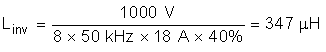
The primary component is the inverter inductor, or Linv, which can be derived using Equation 49:

Equation 1. GUID-3357DE39-B3DB-47B0-B36C-A320D3A920D7-low.gif

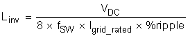
Using re-determined system specifications, one can easily calculate the primary inductor value:

Equation 2. GUID-D9FB570F-5F4E-41B9-9345-CBB9C66E4985-low.gif

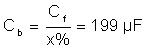
The sizing of the primary filter capacitor is handled in a similar fashion using Equation 3:

Equation 3. GUID-FB7CCE68-481C-423E-805E-CD1EEC5F9F5F-low.gif

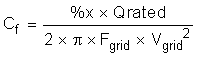
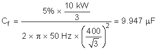
Make some design assumptions to finalize the value of Cf , namely, limiting the total reactive power absorbed by the capacitor to 5%. Scaling the total system power by the per phase power results in a primary capacitor value of:

Equation 4. GUID-C379DB87-3644-47B3-A319-E04FF6B0F218-low.gif
Equation 5. GUID-5369F0F5-AC95-42CC-9D3A-8DE090EB1823-low.gif
Equation 6. GUID-2993B85D-C560-4FE0-BE20-1FA0232C67B2-low.gif

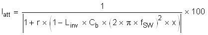
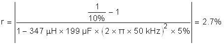
For the remainder of the filter design, determine the values by defining the attenuation factor between the allowable ripple in grid inductor and the inverter inductor. This factor needs to be minimized while still maintaining a stable and cost effective total filter. By assuming an attenuation factor, an r value, which defines the ratio between the two inductors, is determined using Equation 4:

To obtain an attenuation factor of 10%, and using the earlier derived values, the value of r can be evaluated to be:

Equation 7. GUID-3330E7CF-084E-4FAC-B3FA-1E57848693C9-low.gif

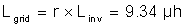
The resultant value for Lgrid is then:

Equation 8. GUID-BB2180BD-41BC-4775-87E7-359158428ED8-low.gif

The filter design can be validated by determining its resonant frequency (Fres). A good criteria for providing a stable Fres is that it is an order of magnitude above the line frequency and less than half the switching frequency. This criteria avoids issues in the upper and lower harmonic spectrums. The resonant frequency of the filter is defined using Equation 9:

Equation 9. GUID-95F3555F-E220-4FC6-9A91-68B4698F6656-low.gif

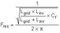
Or, using the derived filter values:

Equation 10. GUID-CE0EB9CE-D888-43BF-A2A8-E9D943485CBC-low.gif

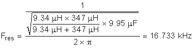
This value for Fres meets the criteria listed earlier and validates the filter design.

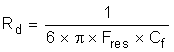
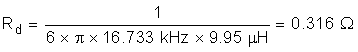
The remaining value to determine is the passive damping that must be added to avoid oscillation. Generally, a damping resistor at the same relative order of magnitude as the Cf impedance at resonance is suitable. This impedance is easily derived using Equation 11:

Equation 11. GUID-3F1AA896-EAB2-493C-B691-691FF12AEE7E-low.gif
Equation 12. GUID-B416E1CB-5903-46A5-9351-B9073857F2DC-low.gif

For the final implementation in hardware, use real values for all of these components based on product availability and must be chosen to be appropriately close (±10% typically). When final values are determined, recalculate the resonant frequency to make sure the filter is still stable.