TIDUE53I march   2018  – july 2023 TMS320F28P550SJ , TMS320F28P559SJ-Q1


  1.   1
  2.   Description
  3.   Resources
  4.   Features
  5.   Applications
  6.   6
  7. 1System Description
    1. 1.1 Key System Specifications
  8. 2System Overview
    1. 2.1 Block Diagram
    2. 2.2 Highlighted Products
      1. 2.2.1  UCC21710
      2. 2.2.2  UCC5320
      3. 2.2.3  TMS320F28379D
      4. 2.2.4  AMC1305M05
      5. 2.2.5  OPA4340
      6. 2.2.6  LM76003
      7. 2.2.7  PTH08080W
      8. 2.2.8  TLV1117
      9. 2.2.9  OPA350
      10. 2.2.10 UCC14240
    3. 2.3 System Design Theory
      1. 2.3.1 Three-Phase T-Type Inverter
        1. 2.3.1.1 Architecture Overview
        2. 2.3.1.2 LCL Filter Design
        3. 2.3.1.3 Inductor Design
        4. 2.3.1.4 SiC MOSFETs Selection
        5. 2.3.1.5 Loss Estimations
        6. 2.3.1.6 Thermal Considerations
      2. 2.3.2 Voltage Sensing
      3. 2.3.3 Current Sensing
      4. 2.3.4 System Power Supplies
        1. 2.3.4.1 Main Input Power Conditioning
        2. 2.3.4.2 Isolated Bias Supplies
      5. 2.3.5 Gate Drivers
        1. 2.3.5.1 1200-V SiC MOSFETs
        2. 2.3.5.2 650-V SiC MOSFETs
        3. 2.3.5.3 Gate Driver Bias Supply
      6. 2.3.6 Control Design
        1. 2.3.6.1 Current Loop Design
        2. 2.3.6.2 PFC DC Bus Voltage Regulation Loop Design
  9. 3Hardware, Software, Testing Requirements, and Test Results
    1. 3.1 Required Hardware and Software
      1. 3.1.1 Hardware
        1. 3.1.1.1 Test Hardware Required
        2. 3.1.1.2 Microcontroller Resources Used on the Design (TMS320F28379D)
        3. 3.1.1.3 F28377D, F28379D Control-Card Settings
        4. 3.1.1.4 Microcontroller Resources Used on the Design (TMS320F280039C)
      2. 3.1.2 Software
        1. 3.1.2.1 Getting Started With Firmware
          1. 3.1.2.1.1 Opening the CCS project
          2. 3.1.2.1.2 Digital Power SDK Software Architecture
          3. 3.1.2.1.3 Interrupts and Lab Structure
          4. 3.1.2.1.4 Building, Loading and Debugging the Firmware
        2. 3.1.2.2 Protection Scheme
        3. 3.1.2.3 PWM Switching Scheme
        4. 3.1.2.4 ADC Loading
    2. 3.2 Testing and Results
      1. 3.2.1 Lab 1
      2. 3.2.2 Testing Inverter Operation
        1. 3.2.2.1 Lab 2
        2. 3.2.2.2 Lab 3
        3. 3.2.2.3 Lab 4
      3. 3.2.3 Testing PFC Operation
        1. 3.2.3.1 Lab 5
        2. 3.2.3.2 Lab 6
        3. 3.2.3.3 Lab 7
      4. 3.2.4 Test Setup for Efficiency
      5. 3.2.5 Test Results
        1. 3.2.5.1 PFC Mode - 230 VRMS, 400 V L-L
          1. 3.2.5.1.1 PFC Start-up – 230 VRMS, 400 L-L AC Voltage
          2. 3.2.5.1.2 Steady State Results at 230 VRMS, 400 V L-L - PFC Mode
          3. 3.2.5.1.3 Efficiency and THD Results at 220 VRMS, 50 Hz – PFC Mode
          4. 3.2.5.1.4 Transient Test With Step Load Change
        2. 3.2.5.2 PFC Mode - 120 VRMS, 208 V L-L
          1. 3.2.5.2.1 Steady State Results at 120 VRMS, 208 V-L-L - PFC Mode
          2. 3.2.5.2.2 Efficiency and THD Results at 120 VRMS - PFC Mode
        3. 3.2.5.3 Inverter Mode
          1. 3.2.5.3.1 Inverter Closed Loop Results
          2. 3.2.5.3.2 Efficiency and THD Results - Inverter Mode
          3. 3.2.5.3.3 Inverter - Transient Test
      6. 3.2.6 Open Loop Inverter Test Results
  10. 4Design Files
    1. 4.1 Schematics
    2. 4.2 Bill of Materials
    3. 4.3 PCB Layout Recommendations
      1. 4.3.1 Layout Prints
    4. 4.4 Altium Project
    5. 4.5 Gerber Files
    6. 4.6 Assembly Drawings
  11. 5Trademarks
  12. 6About the Authors
  13. 7Revision History

Testing PFC Operation

Labs 5, 6, and 7 elaborate the steps for running the power stage in the PFC mode. Lab 5 is the PFC mode of operation in open loop, Lab 6 is the PFC mode of operation with closed current loop. Lab 7 is the PFC mode of operation in closed voltage and current loop and this will be checked both on the HIL platform and actual hardware.

A check for DC bus overvoltage is added to all PFC Labs, Lab 5 through Lab 7, using a filtered value of the DC bus voltage. The TINV_filterAndCheckForBusOverVoltage() function runs from ISR1 and checks for DC bus overvoltage condition. Under OV condition this function shuts off all PWM outputs and registers the system operating state as “bus over-voltage state”. Filtered DC bus voltage is calculated from instantaneous sensed DC bus voltage using the averaging function EMAVG. This is all calculated inside ISR1.

The feed-forward and decoupling function is implemented inside ISR1 and added for all PFC Labs that use a current loop. Therefore, for the PFC mode, this is done in Lab 6 and Lab 7. For this feed-forward and decoupling function filtered DC bus voltage is compared against a user-defined minimum bus voltage to calculate a clamped filtered DC bus voltage. This is also done inside ISR1. This clamped filtered DC bus voltage and the current controller output are finally used to implement the feed-forward and decoupling function.

For SDFM-based current sensing, overcurrent protection (OCP) is also added for all PFC labs.

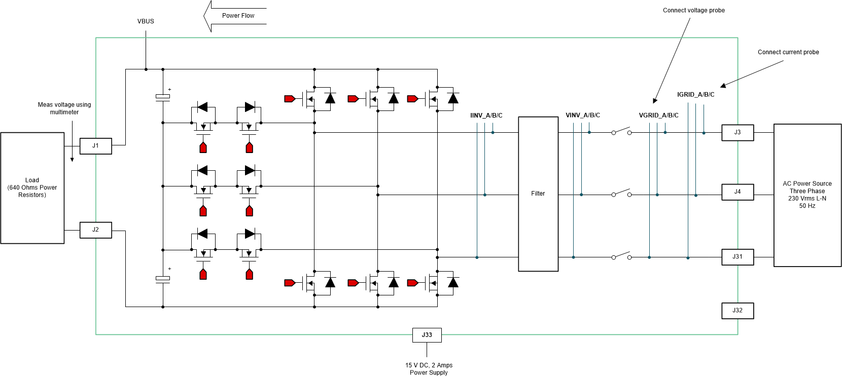
Figure 3-17 shows the hardware setup, the DC terminals J1 and J2 are connected to a resistive load. A 15-V auxiliary power supply is connected to terminal J33. Three phase AC source is connected across terminals J3, J4, and J31 (A, B, and C). J32 is the neutral terminal which is left unconnected to the source. See the hardware test set up section for actual details of the equipment used for configuring the test.
GUID-20210222-CA0I-NK5B-DBQR-KGPPXNVHTNJD-low.gif Figure 3-17 PFC Mode Test Setup