TIDUE53I march 2018 – july 2023 TMS320F28P550SJ , TMS320F28P559SJ-Q1
- 1
- Description
- Resources
- Features
- Applications
- 6
- 1System Description
- 2System Overview
-
3Hardware, Software, Testing Requirements, and Test Results
- 3.1 Required Hardware and Software
- 3.2 Testing and Results
- 4Design Files
- 5Trademarks
- 6About the Authors
- 7Revision History
2.2.3 TMS320F28379D
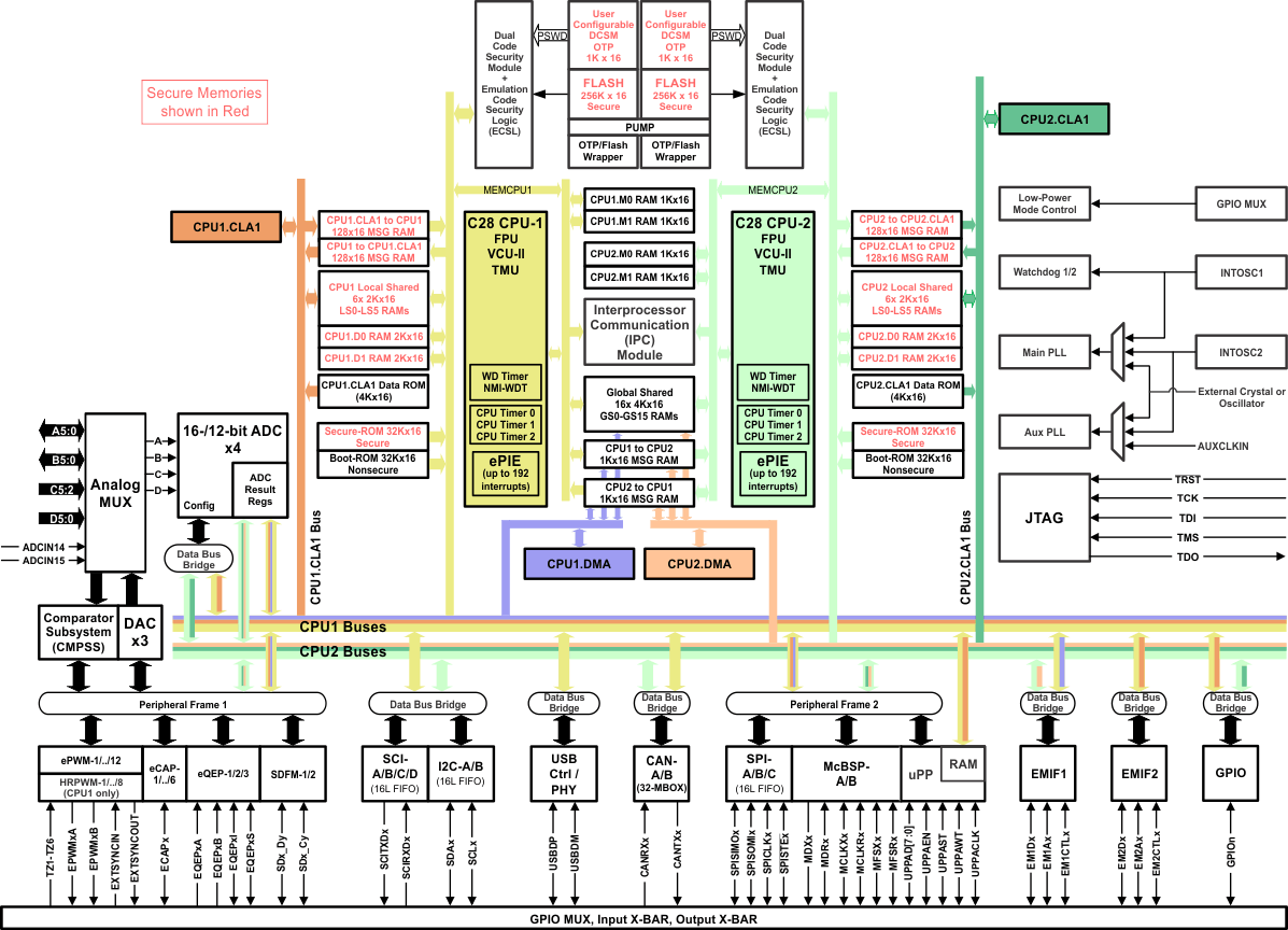
The Delfino™ TMS320F2837xD is a powerful 32-bit floating-point microcontroller unit (MCU) designed for advanced closed-loop control applications such as industrial drives and servo motor control; solar inverters and converters; digital power; transportation; and power line communications. Complete development packages for digital power and industrial drives are available as part of the powerSUITE and DesignDRIVE initiatives. While the Delfino product line is not new to the TMS320C2000™ portfolio, the F2837xD supports a new dual-core C28x architecture that significantly boosts system performance. The integrated analog and control peripherals also let designers consolidate control architectures and eliminate multiprocessor use in high-end systems.
- Dual-core architecture:
- Two TMS320C28x 32-bit CPUs
- 200 MHz
- IEEE 754 single-precision floating-point unit (FPU)
- Trigonometric math unit (TMU)
- Viterbi/complex math unit (VCU-II)
- Two programmable control law accelerators (CLAs)
- 200 MHz
- IEEE 754 single-precision floating-point instructions
- Executes code independently of main CPU
- On-chip memory
- 512KB (256 kW) or 1MB (512 kW) of Flash (ECC-protected)
- 172KB (86 kW) or 204KB (102 kW) of RAM (ECC-protected or parity-protected)
- Dual-zone security supporting third-party development
- Clock and system control:
- Two internal zero-pin 10-MHz oscillators
- On-chip crystal oscillator
- Windowed watchdog timer module
- Missing clock detection circuitry
- 1.2-V core, 3.3-V I/O design
- System peripherals:
- Two external memory interfaces (EMIFs) with ASRAM and SDRAM support
- Dual six-channel direct memory access (DMA) controllers
- Up to 169 individually programmable, multiplexed general-purpose input/output (GPIO) pins with input filtering
- Expanded peripheral interrupt controller (ePIE)
- Multiple low-power mode (LPM) support with external wakeup
- Communications peripherals:
- USB 2.0 (MAC + PHY)
- Support for 12-pin 3.3-V compatible universal parallel port (uPP) interface
- Two controller area network (CAN) modules (pin-bootable)
- Three high-speed (up to 50-MHz) SPI ports (pin-bootable)
- Two multichannel buffered serial ports (McBSPs)
- Four serial communications interfaces (SCI/UART) (pin-bootable)
- Two I2C interfaces (pin-bootable)
- Analog subsystem:
- Up to four analog-to-digital converters (ADCs):
- 16-bit mode
- 1.1 MSPS each (up to 4.4-MSPS system throughput)
- Differential inputs
- Up to 12 external channels
- 12-bit mode
- 3.5 MSPS each (up to 14-MSPS system throughput)
- Single-ended inputs
- Up to 24 external channels
- Single sample-and-hold (S/H) on each ADC
- Hardware-integrated post-processing of ADC conversions:
- Saturating offset calibration
- Error from setpoint calculation
- High, low, and zero-crossing compare, with interrupt capability
- Trigger-to-sample delay capture
- 16-bit mode
- Eight windowed comparators with 12-bit digital-to-analog converter (DAC) references
- Three 12-bit buffered DAC outputs
- Up to four analog-to-digital converters (ADCs):
- Enhanced control peripherals:
- 24 pulse width modulator (PWM) channels with enhanced features
- 16 high-resolution pulse width modulator (HRPWM) channels:
- High resolution on both A and B channels of eight PWM modules
- Dead-band support (on both standard and high resolution)
- Six enhanced capture (eCAP) modules
- Three enhanced quadrature encoder pulse (eQEP) modules
- Eight sigma-delta filter module (SDFM) input channels, two parallel filters per channel:
- Standard SDFM data filtering
- Comparator filter for fast action for out of range
 Figure 2-4 TMS320F28379D Functional Block
Diagram