TIDUE53I march   2018  – july 2023 TMS320F28P550SJ , TMS320F28P559SJ-Q1


  1.   1
  2.   Description
  3.   Resources
  4.   Features
  5.   Applications
  6.   6
  7. 1System Description
    1. 1.1 Key System Specifications
  8. 2System Overview
    1. 2.1 Block Diagram
    2. 2.2 Highlighted Products
      1. 2.2.1  UCC21710
      2. 2.2.2  UCC5320
      3. 2.2.3  TMS320F28379D
      4. 2.2.4  AMC1305M05
      5. 2.2.5  OPA4340
      6. 2.2.6  LM76003
      7. 2.2.7  PTH08080W
      8. 2.2.8  TLV1117
      9. 2.2.9  OPA350
      10. 2.2.10 UCC14240
    3. 2.3 System Design Theory
      1. 2.3.1 Three-Phase T-Type Inverter
        1. 2.3.1.1 Architecture Overview
        2. 2.3.1.2 LCL Filter Design
        3. 2.3.1.3 Inductor Design
        4. 2.3.1.4 SiC MOSFETs Selection
        5. 2.3.1.5 Loss Estimations
        6. 2.3.1.6 Thermal Considerations
      2. 2.3.2 Voltage Sensing
      3. 2.3.3 Current Sensing
      4. 2.3.4 System Power Supplies
        1. 2.3.4.1 Main Input Power Conditioning
        2. 2.3.4.2 Isolated Bias Supplies
      5. 2.3.5 Gate Drivers
        1. 2.3.5.1 1200-V SiC MOSFETs
        2. 2.3.5.2 650-V SiC MOSFETs
        3. 2.3.5.3 Gate Driver Bias Supply
      6. 2.3.6 Control Design
        1. 2.3.6.1 Current Loop Design
        2. 2.3.6.2 PFC DC Bus Voltage Regulation Loop Design
  9. 3Hardware, Software, Testing Requirements, and Test Results
    1. 3.1 Required Hardware and Software
      1. 3.1.1 Hardware
        1. 3.1.1.1 Test Hardware Required
        2. 3.1.1.2 Microcontroller Resources Used on the Design (TMS320F28379D)
        3. 3.1.1.3 F28377D, F28379D Control-Card Settings
        4. 3.1.1.4 Microcontroller Resources Used on the Design (TMS320F280039C)
      2. 3.1.2 Software
        1. 3.1.2.1 Getting Started With Firmware
          1. 3.1.2.1.1 Opening the CCS project
          2. 3.1.2.1.2 Digital Power SDK Software Architecture
          3. 3.1.2.1.3 Interrupts and Lab Structure
          4. 3.1.2.1.4 Building, Loading and Debugging the Firmware
        2. 3.1.2.2 Protection Scheme
        3. 3.1.2.3 PWM Switching Scheme
        4. 3.1.2.4 ADC Loading
    2. 3.2 Testing and Results
      1. 3.2.1 Lab 1
      2. 3.2.2 Testing Inverter Operation
        1. 3.2.2.1 Lab 2
        2. 3.2.2.2 Lab 3
        3. 3.2.2.3 Lab 4
      3. 3.2.3 Testing PFC Operation
        1. 3.2.3.1 Lab 5
        2. 3.2.3.2 Lab 6
        3. 3.2.3.3 Lab 7
      4. 3.2.4 Test Setup for Efficiency
      5. 3.2.5 Test Results
        1. 3.2.5.1 PFC Mode - 230 VRMS, 400 V L-L
          1. 3.2.5.1.1 PFC Start-up – 230 VRMS, 400 L-L AC Voltage
          2. 3.2.5.1.2 Steady State Results at 230 VRMS, 400 V L-L - PFC Mode
          3. 3.2.5.1.3 Efficiency and THD Results at 220 VRMS, 50 Hz – PFC Mode
          4. 3.2.5.1.4 Transient Test With Step Load Change
        2. 3.2.5.2 PFC Mode - 120 VRMS, 208 V L-L
          1. 3.2.5.2.1 Steady State Results at 120 VRMS, 208 V-L-L - PFC Mode
          2. 3.2.5.2.2 Efficiency and THD Results at 120 VRMS - PFC Mode
        3. 3.2.5.3 Inverter Mode
          1. 3.2.5.3.1 Inverter Closed Loop Results
          2. 3.2.5.3.2 Efficiency and THD Results - Inverter Mode
          3. 3.2.5.3.3 Inverter - Transient Test
      6. 3.2.6 Open Loop Inverter Test Results
  10. 4Design Files
    1. 4.1 Schematics
    2. 4.2 Bill of Materials
    3. 4.3 PCB Layout Recommendations
      1. 4.3.1 Layout Prints
    4. 4.4 Altium Project
    5. 4.5 Gerber Files
    6. 4.6 Assembly Drawings
  11. 5Trademarks
  12. 6About the Authors
  13. 7Revision History
Efficiency and THD Results at 220 VRMS, 50 Hz – PFC Mode

This section covers the efficiency and THD results for the converter operating in PFC mode at 220 VRMS. Table 3-8 summarizes the results obtained from power analyzer results when the load is varied from 200 W to 5 kW and DC bus voltage is kept constant at 800 V.

Table 3-8 Detailed Test Results With 220 VAC IN, 800-V DC OUT, and Varying Power Levels
PHASE - A
VOLTAGE
PHASE - B
VOLTAGE
PHASE - C
CURRENT
PHASE - A
CURRENT (A)
PHASE - B
CURRENT
PHASE - C
CURRENT
OUTPUT
DC CURRENT (A)
OUTPUT
POWER (W)

220.3

219.94

220.15

0.398

0.573

0.405

0.25

200

220.1

219.98

220.04

0.974

1.124

0.97

0.753

600

220.09

220.02

219.98

2.55

2.64

2.48

2.018

1610

220.02

219.94

219.93

4.142

4.166

4.016

3.283

2619

220.01

219.97

219.94

5.281

5.262

5.111

4.182

3337

219.92

219.94

219.86

7.325

7.231

7.079

5.793

4624

220.01

219.97

220.03

7.89

7.81

7.76

6.278

5023

OUTPUT


POWER (W)

EFFICIENCY (%)

CURRENT-THD (PHASE-A)CURRENT-THD (PHASE-B)CURRENT-THD (PHASE-C)PFC- (PHASE-A)PFC- (PHASE-B)FC- (PHASE-C)

200

80.93

38.88

55.46

53.44

0.8098

0.8395

0.7934

600

92.06

13.22

23.44

18.54

0.9706

0.9621

0.9678

1610

96.06

5.26

9.59

6.89

0.9944

0.9923

0.9949

2619

96.9

3.09

5.63

4.53

0.9975

0.9968

0.9977

3337

97.11

2.33

4.32

3.66

0.9982

0.9978

0.9985

4624

97.29

1.724

3.034

2.712

0.9988

0.9987

0.9990

5023

97.37

1.47

2.76

1.98

0.9992

0.9991

0.9995

Figure 3-38, Figure 3-49, and Figure 3-50 show the efficiency, THD, and power factor under different load conditions.
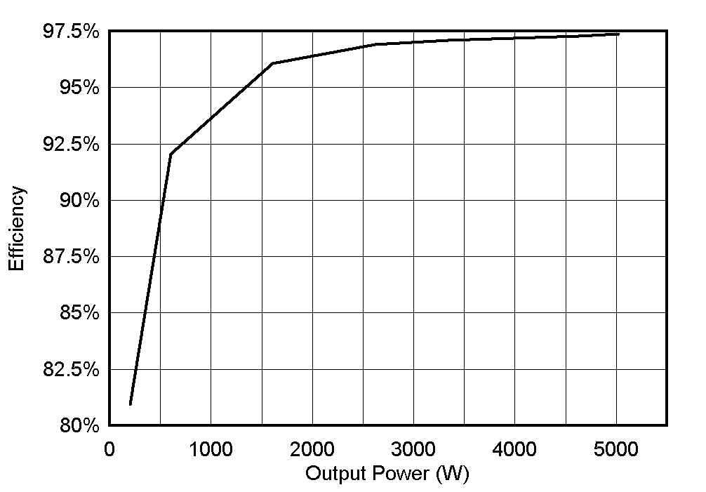
GUID-20210408-CA0I-BDV0-CCS5-32TJJFBBZXXL-low.gifFigure 3-38 Efficiency Results - PFC Mode at 220 VRMS
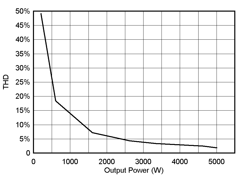
GUID-20210408-CA0I-19N7-DSN4-8HQD4JFR23HG-low.gifFigure 3-39 THD Results - PFC Mode at 220 VRMS
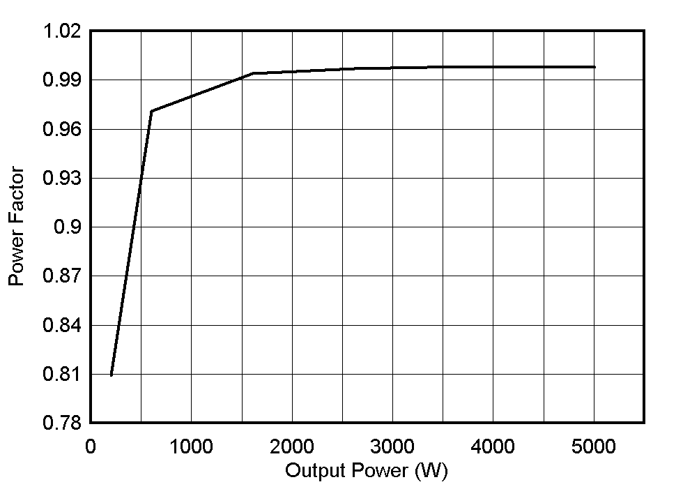
GUID-20210408-CA0I-NWVK-VM6D-4C67B0HPBV28-low.gifFigure 3-40 Power Factor Results - PFC Mode at 220 VRMS

Figure 3-41 shows thermal performance of the board at 4.7 kW.
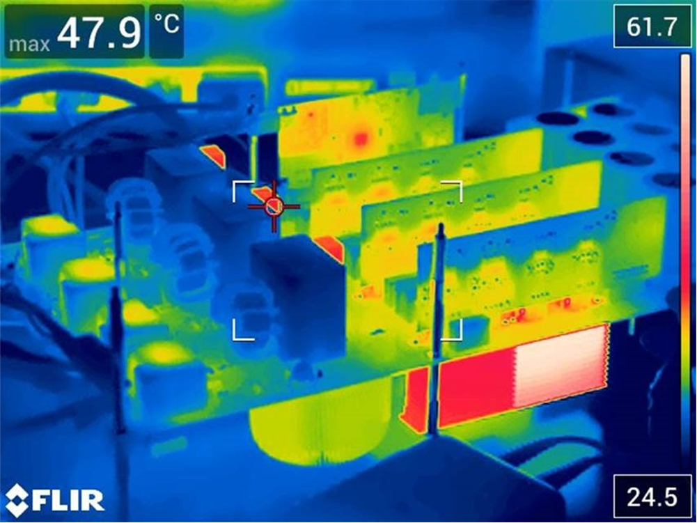
GUID-20210408-CA0I-T0BM-WRPK-C4JWRL1STFLN-low.pngFigure 3-41 Thermal Image at 4.7 kW