SBAS559A May 2022 – December 2022 ADS1285
PRODUCTION DATA
- 1 Features
- 2 Applications
- 3 Description
- 4 Revision History
- 5 Pin Configuration and Functions
-
6 Specifications
- 6.1 Absolute Maximum Ratings
- 6.2 ESD Ratings
- 6.3 Recommended Operating Conditions
- 6.4 Thermal Information
- 6.5 Electrical Characteristics
- 6.6 Timing Requirements: 1.65 V ≤ IOVDD ≤ 1.95 V and 2.7 V ≤ IOVDD ≤ 3.6 V
- 6.7 Switching Characteristics: 1.65V ≤ IOVDD ≤ 1.95V and 2.7 V ≤ IOVDD ≤ 3.6 V
- 6.8 Timing Diagrams
- 6.9 Typical Characteristics
- 7 Parameter Measurement Information
-
8 Detailed Description
- 8.1 Overview
- 8.2 Functional Block Diagram
- 8.3 Feature Description
- 8.4 Device Functional Modes
- 8.5
Programming
- 8.5.1 Serial Interface
- 8.5.2 Conversion Data Format
- 8.5.3
Commands
- 8.5.3.1 Single Byte Command
- 8.5.3.2 WAKEUP: Wake Command
- 8.5.3.3 STANDBY: Software Power-Down Command
- 8.5.3.4 SYNC: Synchronize Command
- 8.5.3.5 RESET: Reset Command
- 8.5.3.6 Read Data Direct
- 8.5.3.7 RDATA: Read Conversion Data Command
- 8.5.3.8 RREG: Read Register Command
- 8.5.3.9 WREG: Write Register Command
- 8.5.3.10 OFSCAL: Offset Calibration Command
- 8.5.3.11 GANCAL: Gain Calibration Command
- 8.6
Register Map
- 8.6.1
Register Descriptions
- 8.6.1.1 ID/SYNC: Device ID, SYNC Register (Address = 00h) [Reset = xxxx0000b]
- 8.6.1.2 CONFIG0: Configuration Register 0 (Address = 01h) [Reset = 12h]
- 8.6.1.3 CONFIG1: Configuration Register 1 (Address = 02h) [Reset = 00h]
- 8.6.1.4 HPF0, HPF1: High-Pass Filter Registers (Address = 03h, 04h) [Reset = 32h, 03h]
- 8.6.1.5 OFFSET0, OFFSET1, OFFSET2: Offset Calibration Registers (Address = 05h, 06h, 07h) [Reset = 00h, 00h, 00h]
- 8.6.1.6 GAIN0, GAIN1, GAIN2: Gain Calibration Registers (Address = 08h, 09h, 0Ah) [Reset = 00h, 00h, 40h]
- 8.6.1.7 GPIO: Digital Input/Output Register (Address = 0Bh) [Reset = 000xx000b]
- 8.6.1.8 SRC0, SRC1: Sample Rate Converter Registers (Address = 0Ch, 0Dh) [Reset = 00h, 80h]
- 8.6.1
Register Descriptions
- 9 Application and Implementation
- 10Device and Documentation Support
- 11Mechanical, Packaging, and Orderable Information
Package Options
Mechanical Data (Package|Pins)
- RHB|32
Thermal pad, mechanical data (Package|Pins)
- RHB|32
Orderable Information
8.3.1 Analog Input
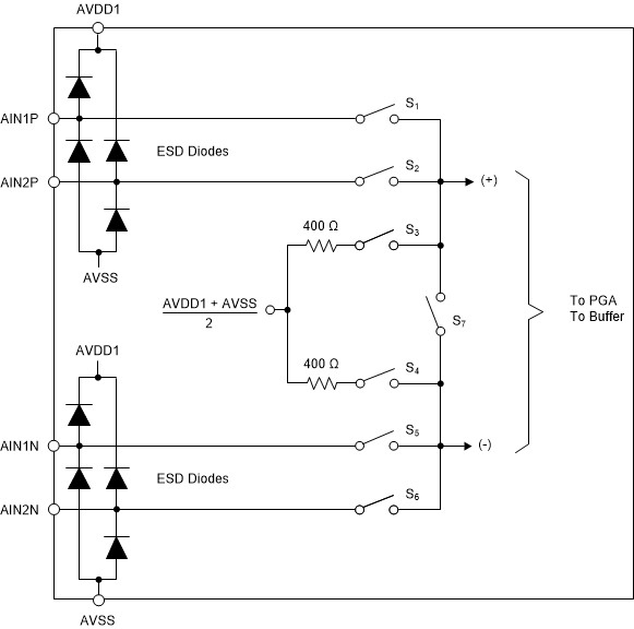
Figure 8-1 shows the analog input circuit and input multiplexer.
 Figure 8-1 Analog Input and
Multiplexer
Figure 8-1 Analog Input and
MultiplexerElectrostatic discharge (ESD) diodes are incorporated to protect the ADC inputs from ESD events that occur during device manufacturing and printed circuit board (PCB) assembly process when assembled in an ESD-controlled environment. For system-level protection, consider using external ESD protection devices to protect the input that are exposed to ESD events.
If the inputs are driven below AVSS – 0.3 V, or above AVDD1 + 0.3 V, the protection diodes can conduct. If these conditions are possible, use external clamp diodes, series resistors, or both to limit input current to the specified maximum value. Overdriving an unused input channel can affect the conversion results of the active input channel. Clamp the overdriven voltage with Schottky diodes to prevent channel crosstalk.
The ADC incorporates two differential input channels The multiplexer selects between the two differential inputs for measurement. A test mode to measure noise and offset is also provided by the multiplexer. The shorted input test configuration is available with or without the 400-Ω resistors to simulate the thermal noise generated by an 800-Ω geophone. Table 8-1 summarizes the multiplexer configurations.
| MUX[2:0] BITS | SWITCHES | DESCRIPTION |
|---|---|---|
| 000 | S1, S5 | Input AIN1P, AIN1N connection |
| 001 | S2, S6 | Input AIN2P, AIN2N connection |
| 010 | S3, S4 | 400-Ω input-short test mode for offset and noise test. |
| 011 | S1, S5,S2, S6 | Cross-connection test mode. Inputs AIN1P, AIN2P and AIN2P, AIN2N are connected |
| 100 | — | Reserved |
| 101 | S3,S4,S7 | 0-Ω input-short test mode for offset and noise test. |
To test geophone THD performance, apply a test signal to the test channel through series resistors. The series resistors are typically half the value of the geophone impedance. Select the multiplexer for the cross-connection test mode (MUX[2:0] = 011b). In cross-connection mode, the test signal is cross-fed to the geophone input.
Geophone THD test performance can be affected by the nonlinear on-resistance of the multiplexer (RSW). Figure 8-2 shows a model of the input multiplexer resistance for the geophone THD test. Figure 8-3 shows THD performance versus a test resistor (RLOAD) used to simulate geophone resistance. Small amplitude test signals (such as, VIN = 0.221 V), shows less THD performance degradation for geophone resistance < 500 Ω.