SBAS559A May 2022 – December 2022 ADS1285
PRODUCTION DATA
- 1 Features
- 2 Applications
- 3 Description
- 4 Revision History
- 5 Pin Configuration and Functions
-
6 Specifications
- 6.1 Absolute Maximum Ratings
- 6.2 ESD Ratings
- 6.3 Recommended Operating Conditions
- 6.4 Thermal Information
- 6.5 Electrical Characteristics
- 6.6 Timing Requirements: 1.65 V ≤ IOVDD ≤ 1.95 V and 2.7 V ≤ IOVDD ≤ 3.6 V
- 6.7 Switching Characteristics: 1.65V ≤ IOVDD ≤ 1.95V and 2.7 V ≤ IOVDD ≤ 3.6 V
- 6.8 Timing Diagrams
- 6.9 Typical Characteristics
- 7 Parameter Measurement Information
-
8 Detailed Description
- 8.1 Overview
- 8.2 Functional Block Diagram
- 8.3 Feature Description
- 8.4 Device Functional Modes
- 8.5
Programming
- 8.5.1 Serial Interface
- 8.5.2 Conversion Data Format
- 8.5.3
Commands
- 8.5.3.1 Single Byte Command
- 8.5.3.2 WAKEUP: Wake Command
- 8.5.3.3 STANDBY: Software Power-Down Command
- 8.5.3.4 SYNC: Synchronize Command
- 8.5.3.5 RESET: Reset Command
- 8.5.3.6 Read Data Direct
- 8.5.3.7 RDATA: Read Conversion Data Command
- 8.5.3.8 RREG: Read Register Command
- 8.5.3.9 WREG: Write Register Command
- 8.5.3.10 OFSCAL: Offset Calibration Command
- 8.5.3.11 GANCAL: Gain Calibration Command
- 8.6
Register Map
- 8.6.1
Register Descriptions
- 8.6.1.1 ID/SYNC: Device ID, SYNC Register (Address = 00h) [Reset = xxxx0000b]
- 8.6.1.2 CONFIG0: Configuration Register 0 (Address = 01h) [Reset = 12h]
- 8.6.1.3 CONFIG1: Configuration Register 1 (Address = 02h) [Reset = 00h]
- 8.6.1.4 HPF0, HPF1: High-Pass Filter Registers (Address = 03h, 04h) [Reset = 32h, 03h]
- 8.6.1.5 OFFSET0, OFFSET1, OFFSET2: Offset Calibration Registers (Address = 05h, 06h, 07h) [Reset = 00h, 00h, 00h]
- 8.6.1.6 GAIN0, GAIN1, GAIN2: Gain Calibration Registers (Address = 08h, 09h, 0Ah) [Reset = 00h, 00h, 40h]
- 8.6.1.7 GPIO: Digital Input/Output Register (Address = 0Bh) [Reset = 000xx000b]
- 8.6.1.8 SRC0, SRC1: Sample Rate Converter Registers (Address = 0Ch, 0Dh) [Reset = 00h, 80h]
- 8.6.1
Register Descriptions
- 9 Application and Implementation
- 10Device and Documentation Support
- 11Mechanical, Packaging, and Orderable Information
Package Options
Mechanical Data (Package|Pins)
- RHB|32
Thermal pad, mechanical data (Package|Pins)
- RHB|32
Orderable Information
8.3.6.4 HPF Stage
The last stage of the digital filter is the high-pass filter (HPF). The high-pass filter is implemented as a first-order, IIR filter. The high-pass filter removes dc and low frequencies from the data. The HPF is enabled by programming the FILTR[1:0] bits = 11b of the CONFIG0 register.
Equation 4 shows the z-domain transfer function of the filter:
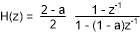
where:
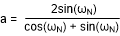
- ωN = π × fC / fDATA (normalized corner frequency, radians)
- fC = Corner frequency (Hz)
- fDATA = Output data rate (Hz)
Be aware the corner frequency programming is a function of fDATA. As shown by Equation 5, the value written to the HPF1, HPF0 registers is value a, computed by Equation 4, × 216.
Table 8-6 shows examples of the high-pass filter programming.
| HPF[15:0] | fC (Hz) | fDATA (SPS) |
|---|---|---|
| 0332h | 0.5 | 250 |
| 0332h | 1.0 | 500 |
| 019Ah | 1.0 | 1000 |
The HPF accumulates data to perform the high-pass function. Similar to the operation of an analog HPF after a dc step change is applied to the input, the filter takes time to accumulate data to remove dc from the signal. The lower the corner frequency, the longer the filter takes to settle.
To shorten the HPF settling time, the offset register is used as a seed value for the HPF accumulator. The accumulator is loaded with the offset register each time the HPF state is changed from disabled to enabled. The offset register can be preset with an estimated value, or a calibrated value if the dc level is known. To improve accuracy, scale the offset value by the inverse value of GAIN[3:0] / 400000h. The normal offset operation is disabled when the HPF is enabled.
To initialize the HPF accumulator with the OFFSET[2:0] registers:
- Disable the HPF.
- Write the desired value to the OFFSET[2:0] registers.
- Enable the HPF. OFFSET[2:0] is loaded to the HPF data accumulator.
- The HPF tracks the remaining dc value from the signal.
Subsequent writes to the OFFSET[2:0] registers are ignored. To reload the contents of the OFFSET[2:0] registers to the HPF, disable and re-enable the HPF.