SBAS603B April 2013 – November 2020 ADS4449
PRODUCTION DATA
- 1 Features
- 2 Applications
- 3 Description
- 4 Revision History
- 5 Pin Configuration and Functions
- 6 Specifications
- 7 Parameter Measurement Information
-
8 Detailed Description
- 8.1 Overview
- 8.2 Functional Block Diagram
- 8.3 Feature Description
- 8.4 Device Functional Modes
- 8.5 Programming
- 8.6
Register Maps
- 8.6.1
Register Description
- 8.6.1.1 Register Address 00h (Default = 00h)
- 8.6.1.2 Register Address 01h (Default = 00h)
- 8.6.1.3 Register Address 25h (Default = 00h)
- 8.6.1.4 Register Address 2bh (Default = 00h)
- 8.6.1.5 Register Address 31h (Default = 00h)
- 8.6.1.6 Register Address 37h (Default = 00h)
- 8.6.1.7 Register Address 3dh (Default = 00h)
- 8.6.1.8 Register Address 3fh (Default = 00h)
- 8.6.1.9 Register Address 40h (Default = 00h)
- 8.6.1.10 Register Address 42h (Default = 00h)
- 8.6.1.11 Register Address 45h (Default = 00h)
- 8.6.1.12 Register Address 4ah (Defalut = 00h)
- 8.6.1.13 Register Address 62h (Default = 00h)
- 8.6.1.14 Register Address 7ah (Default = 00h)
- 8.6.1.15 Register Address 92h (Default = 00h)
- 8.6.1.16 Register Address A9h (Default = 00h)
- 8.6.1.17 Register Address Ach (Default = 00h)
- 8.6.1.18 Register Address C3h (Default = 00h)
- 8.6.1.19 Register Address C4h (Default = 00h)
- 8.6.1.20 Register Address Cfh (Default = 00h)
- 8.6.1.21 Register Address D6h (Default = 00h)
- 8.6.1.22 Register Address D7h (Default = 00h)
- 8.6.1.23 Register Address F1h (Default = 00h)
- 8.6.1.24 Register Address 58h (Default = 00h)
- 8.6.1.25 Register Address 59h (Default = 00h)
- 8.6.1.26 Register Address 70h (Default = 00h)
- 8.6.1.27 Register Address 71h (Default = 00h)
- 8.6.1.28 Register Address 88h (Default = 00h)
- 8.6.1.29 Register Address 89h (Default = 00h)
- 8.6.1.30 Register Address A0h (Default = 00h)
- 8.6.1.31 Register Address A1h (Default = 00h)
- 8.6.1.32 Register Address Feh (Default = 00h)
- 8.6.1
Register Description
- 9 Application and Implementation
- 10Power Supply Recommendations
- 11Layout
- 12Device and Documentation Support
Package Options
Mechanical Data (Package|Pins)
- ZCR|144
Thermal pad, mechanical data (Package|Pins)
Orderable Information
12.1 Device Nomenclature
- Analog BandwidthThe analog input frequency at which the power of the fundamental is reduced by 3 dB with respect to the low-frequency value.
- Aperture DelayThe delay in time between the rising edge of the input sampling clock and the actual time at which the sampling occurs. This delay is different across channels. The maximum variation is specified as an aperture delay variation (channel-to-channel).
- Aperture Uncertainty (Jitter)The sample-to-sample variation in aperture delay.
- Clock Pulse Width and Duty CycleThe duty cycle of a clock signal is the ratio of the time the clock signal remains at a logic high (clock pulse width) to the period of the clock signal. Duty cycle is typically expressed as a percentage. A perfect differential sine-wave clock results in a 50% duty cycle.
- Maximum Conversion RateThe maximum sampling rate at which specified operation is given. All parametric testing is performed at this sampling rate, unless otherwise noted.
- Minimum Conversion RateThe minimum sampling rate at which the ADC functions.
- Differential Nonlinearity (DNL)An ideal ADC exhibits code transitions at analog input values spaced exactly 1 LSB apart. DNL is the deviation of any single step from this ideal value, measured in units of LSBs.
- Integral Nonlinearity (INL)INL is the deviation of the ADC transfer function from a best-fit line determined by a least-squares curve fit of that transfer function, measured in units of LSBs.
- Gain ErrorGain error is the deviation of the ADC actual input full-scale range from the ideal value. Gain error is given as a percentage of the ideal input full-scale range. Gain error has two components: error as a result of reference inaccuracy and error as a result of the channel. Both errors are specified independently as EGREF and EGCHAN.
To a first-order approximation, the total gain error of ETOTAL is approximately EGREF + EGCHAN.
For example, if ETOTAL = ±0.5%, the full-scale input varies from (1 – 0.5 / 100) × fS ideal to (1 + 0.5 / 100) × fS ideal.
- Offset ErrorOffset error is the difference, given in number of LSBs, between the ADC actual average idle channel output code and the ideal average idle channel output code. This quantity is often mapped into millivolts.
- Temperature DriftThe temperature drift coefficient (with respect to gain error and offset error) specifies the change per degree Celsius of the parameter from TMIN to TMAX. The coefficient is calculated by dividing the maximum deviation of the parameter across the TMIN to TMAX range by the difference of TMAX – TMIN.
- Signal-to-Noise Ratio (SNR)SNR is the ratio of the power of the fundamental (PS) to the noise floor power (PN), excluding the power at dc and the first nine harmonics.
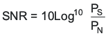
SNR is either given in units of dBc (dB to carrier) when the absolute power of the fundamental is used as the reference, or dBFS (dB to full-scale) when the power of the fundamental is extrapolated to the converter full-scale range.
- Signal-to-Noise and Distortion (SINAD)SINAD is the ratio of the power of the fundamental (PS) to the power of all other spectral components, including noise (PN) and distortion (PD) but excluding dc.
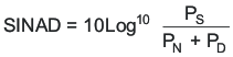
SINAD is either given in units of dBc (dB to carrier) when the absolute power of the fundamental is used as the reference, or dBFS (dB to full-scale) when the power of the fundamental is extrapolated to the converter full-scale range.