SBAS843A september 2017 – july 2023 ADS8588H
PRODUCTION DATA
- 1
- 1 Features
- 2 Applications
- 3 Description
- 4 Revision History
- 5 Pin Configuration and Functions
-
6 Specifications
- 6.1 Absolute Maximum Ratings
- 6.2 ESD Ratings
- 6.3 Recommended Operating Conditions
- 6.4 Thermal Information
- 6.5 Electrical Characteristics
- 6.6 Timing Requirements: CONVST Control
- 6.7 Timing Requirements: Data Read Operation
- 6.8 Timing Requirements: Parallel Data Read Operation, CS and RD Tied Together
- 6.9 Timing Requirements: Parallel Data Read Operation, CS and RD Separate
- 6.10 Timing Requirements: Serial Data Read Operation
- 6.11 Timing Requirements: Byte Mode Data Read Operation
- 6.12 Timing Requirements: Oversampling Mode
- 6.13 Timing Requirements: Exit Standby Mode
- 6.14 Timing Requirements: Exit Shutdown Mode
- 6.15 Switching Characteristics: CONVST Control
- 6.16 Switching Characteristics: Parallel Data Read Operation, CS and RD Tied Together
- 6.17 Switching Characteristics: Parallel Data Read Operation, CS and RD Separate
- 6.18 Switching Characteristics: Serial Data Read Operation
- 6.19 Switching Characteristics: Byte Mode Data Read Operation
- 6.20 Timing Diagrams
- 6.21 Typical Characteristics
-
7 Detailed Description
- 7.1 Overview
- 7.2 Functional Block Diagram
- 7.3 Feature Description
- 7.4
Device Functional Modes
- 7.4.1
Device Interface: Pin Description
- 7.4.1.1 REFSEL (Input)
- 7.4.1.2 RANGE (Input)
- 7.4.1.3 STBY (Input)
- 7.4.1.4 PAR/SER/BYTE SEL (Input)
- 7.4.1.5 CONVSTA, CONVSTB (Input)
- 7.4.1.6 RESET (Input)
- 7.4.1.7 RD/SCLK (Input)
- 7.4.1.8 CS (Input)
- 7.4.1.9 OS[2:0]
- 7.4.1.10 BUSY (Output)
- 7.4.1.11 FRSTDATA (Output)
- 7.4.1.12 DB15/BYTE SEL
- 7.4.1.13 DB14/HBEN
- 7.4.1.14 DB[13:9]
- 7.4.1.15 DB8/DOUTB
- 7.4.1.16 DB7/DOUTA
- 7.4.1.17 DB[6:0]
- 7.4.2 Device Modes of Operation
- 7.4.1
Device Interface: Pin Description
- 8 Application and Implementation
- 9 Device and Documentation Support
- 10Mechanical, Packaging, and Orderable Information
Package Options
Mechanical Data (Package|Pins)
- PM|64
Thermal pad, mechanical data (Package|Pins)
Orderable Information
7.4.2.2.1 Simultaneous Sampling on All Input Channels
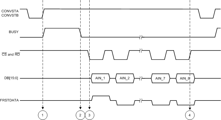
The ADS8588H allows all analog input channels to be simultaneously sampled. In order to do so, the CONVSTA and CONVSTB signals must be tied together as shown in Figure 7-16 and a single CONVST signal must be used to control the sampling of all analog input channels of the device. Figure 7-16 also shows the sequence of events described in this section.
 Figure 7-16 Simultaneous Sampling of All Input Channels in Parallel Interface Timing Diagram
There are four events that describe the internal operation of the device when all input channels are simultaneously sampled and the data are read back. These events are:
- Event 1: Simultaneous sampling of all analog input channels is initiated with the rising edge of the CONVST signal. The input signals on all channels are sampled at this same instant because both the CONVSTA and CONVSTB inputs are tied together. The sampled signals are then converted by the ADCs using a precise on-chip oscillator clock. At the beginning of the conversion phase of the ADC, the BUSY output goes high and remains high through a maximum-specified conversion time of tCONV (see the Timing Requirements: CONVST ControlTiming Requirements: CONVST Control table).
- Event 2: At this instant, the ADC has completed the conversion for all input channels and the BUSY output goes to logic low. The falling edge of the BUSY signal indicates end of conversion and that the internal registers are updated with the conversion data. At this instant, the device is ready to output the correct conversion results for all channels on the parallel output bus (DB[15:0]), serial output lines (DOUTA, DOUTB), or parallel byte bus (DB[7:0]).
- Event 3: This example shows the data read operation in parallel interface mode with both CS and RD tied together. After BUSY goes low, the first falling edges of CS and RD output the conversion result of channel 1 (AIN_1) on the parallel output bus. Similarly, the conversion results for the remaining channels are output on the parallel bus on subsequent falling edges of the CS and RD signals in a sequential manner. If all channels are not used in the conversion process, tie the unused channels to AGND or any known voltage within the selected input range. The ADC always converts all analog input channels and the results for unused channels are included in the output data stream, thus all unused channels must be tied to AGND or a known voltage within the range. The FRSTDATA output goes high on the first falling edges of the CS and RD signals, indicating that the parallel bus is carrying the output result from channel 1. On the next falling edge of the CS and RD signals, FRSTDATA goes low and stays low if the CS and RD inputs are low.
- Event 4: After the conversion results for all analog channels are output from the device, the data frame can be terminated by pulling the CS and RD signals to logic high. The parallel bus and FRSTDATA output go to tri-state until the entire sequence is repeated beginning from event 1.
Events 1 and 2 are common to all interface modes of operation (parallel or serial or parallel byte).