SBAS843A september 2017 – july 2023 ADS8588H
PRODUCTION DATA
- 1
- 1 Features
- 2 Applications
- 3 Description
- 4 Revision History
- 5 Pin Configuration and Functions
-
6 Specifications
- 6.1 Absolute Maximum Ratings
- 6.2 ESD Ratings
- 6.3 Recommended Operating Conditions
- 6.4 Thermal Information
- 6.5 Electrical Characteristics
- 6.6 Timing Requirements: CONVST Control
- 6.7 Timing Requirements: Data Read Operation
- 6.8 Timing Requirements: Parallel Data Read Operation, CS and RD Tied Together
- 6.9 Timing Requirements: Parallel Data Read Operation, CS and RD Separate
- 6.10 Timing Requirements: Serial Data Read Operation
- 6.11 Timing Requirements: Byte Mode Data Read Operation
- 6.12 Timing Requirements: Oversampling Mode
- 6.13 Timing Requirements: Exit Standby Mode
- 6.14 Timing Requirements: Exit Shutdown Mode
- 6.15 Switching Characteristics: CONVST Control
- 6.16 Switching Characteristics: Parallel Data Read Operation, CS and RD Tied Together
- 6.17 Switching Characteristics: Parallel Data Read Operation, CS and RD Separate
- 6.18 Switching Characteristics: Serial Data Read Operation
- 6.19 Switching Characteristics: Byte Mode Data Read Operation
- 6.20 Timing Diagrams
- 6.21 Typical Characteristics
-
7 Detailed Description
- 7.1 Overview
- 7.2 Functional Block Diagram
- 7.3 Feature Description
- 7.4
Device Functional Modes
- 7.4.1
Device Interface: Pin Description
- 7.4.1.1 REFSEL (Input)
- 7.4.1.2 RANGE (Input)
- 7.4.1.3 STBY (Input)
- 7.4.1.4 PAR/SER/BYTE SEL (Input)
- 7.4.1.5 CONVSTA, CONVSTB (Input)
- 7.4.1.6 RESET (Input)
- 7.4.1.7 RD/SCLK (Input)
- 7.4.1.8 CS (Input)
- 7.4.1.9 OS[2:0]
- 7.4.1.10 BUSY (Output)
- 7.4.1.11 FRSTDATA (Output)
- 7.4.1.12 DB15/BYTE SEL
- 7.4.1.13 DB14/HBEN
- 7.4.1.14 DB[13:9]
- 7.4.1.15 DB8/DOUTB
- 7.4.1.16 DB7/DOUTA
- 7.4.1.17 DB[6:0]
- 7.4.2 Device Modes of Operation
- 7.4.1
Device Interface: Pin Description
- 8 Application and Implementation
- 9 Device and Documentation Support
- 10Mechanical, Packaging, and Orderable Information
Package Options
Mechanical Data (Package|Pins)
- PM|64
Thermal pad, mechanical data (Package|Pins)
Orderable Information
7.3.9 ADC Transfer Function
The ADS8588H is a multichannel device that support two single-ended, bipolar input ranges of ±10 V and ±5 V on all input channels. The device outputs 16 bits of conversion data in binary two's complement format for both bipolar input ranges. The format for the output codes is the same across all analog channels.
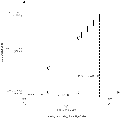
Figure 7-15 shows the ideal transfer characteristic for each ADC channel for all input ranges. The full-scale range (FSR) for each input signal is equal to the difference between the positive full-scale (PFS) input voltage and the negative full-scale (NFS) input voltage. The LSB size is equal to FSR / 216 = FSR / 65536 because the resolution of the ADC is 16 bits. Table 7-2 lists the LSB values corresponding to the different input ranges.
 Figure 7-15 16-Bit ADC Transfer Function (Two's Complement Binary Format)
| INPUT RANGE (V) | POSITIVE FULL-SCALE (V) | NEGATIVE FULL-SCALE (V) | FULL-SCALE RANGE (V) | LSB (µV) |
|---|---|---|---|---|
| ±10 | 10 | –10 | 20 | 305.18 |
| ±5 | 5 | –5 | 10 | 152.59 |