SBOS531E August 2010 – June 2019 AFE031
PRODUCTION DATA.
- 1 Features
- 2 Applications
- 3 Description
- 4 Revision History
- 5 Description, continued
- 6 Device Comparison Table
- 7 Pin Configuration and Functions
-
8 Specifications
- 8.1 Absolute Maximum Ratings
- 8.2 ESD Ratings
- 8.3 Thermal Information
- 8.4 Electrical Characteristics: Transmitter (Tx)
- 8.5 Electrical Characteristics: Power Amplifier (PA)
- 8.6 Electrical Characteristics: Receiver (Rx)
- 8.7 Electrical Characteristics: Digital
- 8.8 Electrical Characteristics: Two-Wire Interface
- 8.9 Electrical Characteristics: Internal Bias Generator
- 8.10 Electrical Characteristics: Power Supply
- 8.11 Timing Requirements
- 8.12 Timing Diagrams
- 8.13 Typical Characteristics
- 9 Detailed Description
- 10Application and Implementation
- 11Device and Documentation Support
- 12Mechanical, Packaging, and Orderable Information
Package Options
Mechanical Data (Package|Pins)
- RGZ|48
Thermal pad, mechanical data (Package|Pins)
- RGZ|48
Orderable Information
10.1 Application Information
The AFE031 is an integrated powerline communication analog front-end (AFE) device built from a variety of functional blocks that work in conjunction with a microcontroller. The AFE031 provides the interface between the microcontroller and a line coupling circuit. The AFE031 delivers high performance and is designed to work with a minimum number of external components. Consisting of a variety of functional and configurable blocks, the AFE031 simplifies design efforts and reduces the time to market of many applications.
The AFE031 includes three primary functional blocks:
- Power Amplifier (PA)
- Transmitter (Tx)
- Receiver (Rx)
The AFE031 also consists of other support circuitry blocks that provide zero crossing detection, an additional two-wire communications channel, and power-saving biasing blocks (see the ). All of these functional blocks are digitally controlled by the microcontroller through the serial interface (SPI).
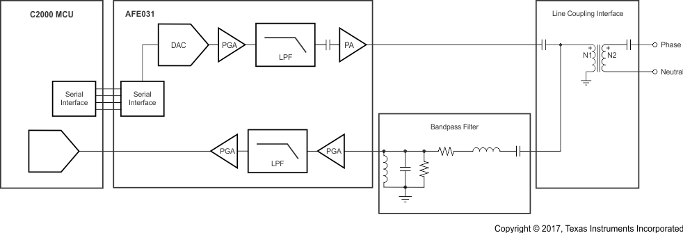
Figure 47 shows a typical powerline communications application system diagram. Table 19 is a complete list of the sections within the AFE031.
 Figure 47. Typical Powerline Communications System Diagram
 Table 19. Block Descriptions
| BLOCK | DESCRIPTION |
|---|---|
| PA | The PA block includes the power amplifier and associated pedestal biasing circuitry |
| Tx | The Tx block includes the Tx_Filter and the Tx_PGA |
| Rx | The Rx block includes the Rx PGA1, the Rx Filter, and the Rx PGA2 |
| ERx | The ER block includes the two-wire receiver |
| ETx | The ER block includes the two-wire transmitter |
| DAC | The DAC block includes a digital-to-analog converter |
| ZC | The ZC block includes both zero crossing detectors |
| REF1 | The REF1 block includes the internal bias generator for the PA block |
| REF2 | The REF2 block includes the internal bias generators for the Tx, Rx, ERx, and ETx blocks |