SBOS531E August 2010 – June 2019 AFE031
PRODUCTION DATA.
- 1 Features
- 2 Applications
- 3 Description
- 4 Revision History
- 5 Description, continued
- 6 Device Comparison Table
- 7 Pin Configuration and Functions
-
8 Specifications
- 8.1 Absolute Maximum Ratings
- 8.2 ESD Ratings
- 8.3 Thermal Information
- 8.4 Electrical Characteristics: Transmitter (Tx)
- 8.5 Electrical Characteristics: Power Amplifier (PA)
- 8.6 Electrical Characteristics: Receiver (Rx)
- 8.7 Electrical Characteristics: Digital
- 8.8 Electrical Characteristics: Two-Wire Interface
- 8.9 Electrical Characteristics: Internal Bias Generator
- 8.10 Electrical Characteristics: Power Supply
- 8.11 Timing Requirements
- 8.12 Timing Diagrams
- 8.13 Typical Characteristics
- 9 Detailed Description
- 10Application and Implementation
- 11Device and Documentation Support
- 12Mechanical, Packaging, and Orderable Information
Package Options
Mechanical Data (Package|Pins)
- RGZ|48
Thermal pad, mechanical data (Package|Pins)
- RGZ|48
Orderable Information
10.2 Typical Application
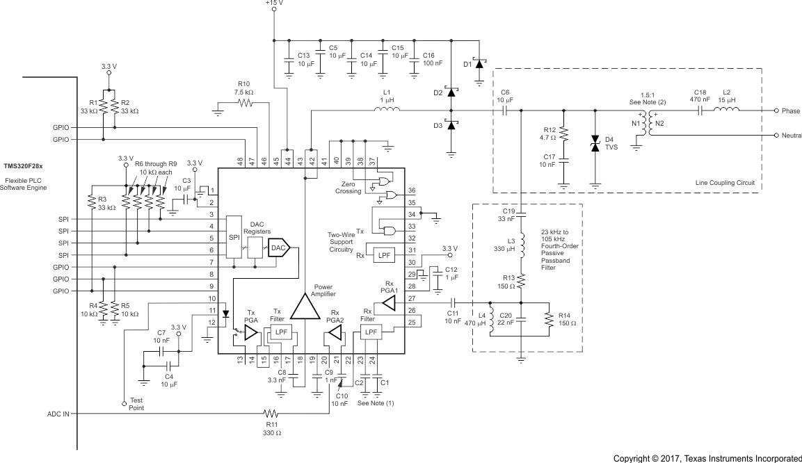
Figure 48 shows the AFE031 configured in a typical PLC analog front-end application. The schematic shows the connections to the microprocessor and ac line. The values of the passive components in Figure 48 are suitable for a single-phase powerline communications application in the CENELEC A band, connected to a 120-VAC or 240-VAC, 50-Hz or 60-Hz ac line.

1. Recommended values for C1 and C2:
Figure 48. Typical Powerline Communications Modem Application - C1:
- CENELEC A: 680 pF
- CENELEC B, C, D: 270 pF
- C2:
- CENELEC A: 680 pF
- CENELEC B, C, D: 560 pF