SBFS042 June 2020 AFE3010
PRODUCTION DATA.
- 1 Features
- 2 Applications
- 3 Description
- 4 Revision History
- 5 Pin Configuration and Functions
- 6 Specifications
- 7 Detailed Description
- 8 Application and Implementation
- 9 Power Supply Recommendations
- 10Layout
- 11Device and Documentation Support
- 12Mechanical, Packaging, and Orderable Information
Package Options
Mechanical Data (Package|Pins)
- RGT|16
Thermal pad, mechanical data (Package|Pins)
- RGT|16
Orderable Information
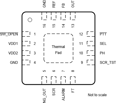
5 Pin Configuration and Functions
RGT Package
16-Pin VQFN
Top View

Pin Functions
| PIN | I/O | DESCRIPTION | |
|---|---|---|---|
| NO. | NAME | ||
| 1 | SW_OPEN | Input | Controls ALARM pin while asserted low. Refer to Table 3 for more details. |
| 2 | VDD1 | Power | Power supply to the part from rectifying diode through series resistor. There is also a decoupling cap at this pin. |
| 3 | VDD2 | Power | Redundant power supply pin. |
| 4 | GND | Ground | Ground pin for the device. |
| 5 | NG_OUT | Output | Generates a pulse to start the Ground to Neutral fault detection scheme. Drives the secondary winding of the 200:1 transformer through an AC-coupled capacitor. Leave this pin floating if Neutral-GND fault detection is not needed. |
| 6 | SCR | Output | Current output pin that drives the SCR after a fault is detected. |
| 7 | ALARM | Output | Alarm/ LED driver output. Drives a 3-KHz signal that can be used to drive an LED or buzzer to indicate that the self-test failed. Can be configured as secondary SCR driver when a 500-KΩ resistor is connected between SEL pin and ground. Refer to Table 2 for more details. |
| 8 | FT | Output | Drives the base of a bipolar transistor to emulate fault event during self-test. |
| 9 | SCR_TST | I/O | Monitors the phase of the sine wave of HOT power line after the solenoid. Drives a weak HIGH output during SCR self-test. Clamped to VDD through an internal diode. |
| 10 | PH | Input | Monitors the phase of the sine wave of HOT power line. Clamped to VDD through an internal diode. |
| 11 | SEL | Input | Control pin to configure the device. Refer to Table 2 for more details. |
| 12 | PTT | Input | Active-low push-to-test pin. Starts self-test and fires SCR if self-test passes. |
| 13 | OUT | Output | Amplifier output node. |
| 14 | FB | Input | Amplifier inverting input. |
| 15 | REF | I/O | Amplifier non-inverting input. Typically 2.5 V derived from an internal 5-V regulator. |
| 16 | GND | Ground | Ground pin for the device. |