SLUSCM2B October 2017 – November 2018
PRODUCTION DATA.
- 1 Features
- 2 Applications
- 3 Description
- 4 Revision History
- 5 Description (continued)
- 6 Device Comparison Table
- 7 Pin Configuration and Functions
- 8 Specifications
-
9 Detailed Description
- 9.1 Overview
- 9.2 Functional Block Diagram
- 9.3 Feature Description
- 9.4 Device Functional Modes
-
10Application and Implementation
- 10.1 Application Information
- 10.2 Typical Application – bq24079QW-Q1 Charger Design Example
- 11Power Supply Recommendations
- 12Layout
- 13Device and Documentation Support
- 14Mechanical, Packaging, and Orderable Information
Package Options
Refer to the PDF data sheet for device specific package drawings
Mechanical Data (Package|Pins)
- RGT|16
Thermal pad, mechanical data (Package|Pins)
- RGT|16
Orderable Information
9.3.5 Battery Charging
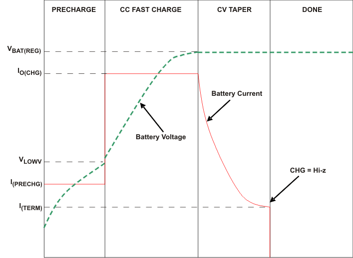
Set CE low to initiate battery charging. First, the device checks for a short-circuit on the BAT pin by sourcing IBAT(SC) to the battery and monitoring the voltage. When the BAT voltage exceeds VBAT(SC), the battery charging continues. The battery is charged in three phases: conditioning pre-charge, constant current fast charge (current regulation) and a constant voltage tapering (voltage regulation). In all charge phases, an internal control loop monitors the IC junction temperature and reduces the charge current if an internal temperature threshold is exceeded.
Figure 22 illustrates a normal Li-Ion charge cycle using the bq24079QW-Q1:
 Figure 22. Typical Charge Cycle
 In the pre-charge phase, the battery is charged with the pre-charge current (IPRECHG). Once the battery voltage crosses the VLOWV threshold, the battery is charged with the fast-charge current (ICHG). As the battery voltage reaches VBAT(REG), the battery is held at a constant voltage of VBAT(REG) and the charge current tapers off as the battery approaches full charge. When the battery current reaches ITERM, the CHG pin indicates charging done by going high-impedance.
Note that termination detection is disabled whenever the charge rate is reduced because of the actions of the thermal loop, the DPPM loop or the VIN(LOW) loop.
The value of the fast-charge current is set by the resistor connected from the ISET pin to VSS, and is given by the equation:
The charge current limit is adjustable up to 1.5 A. The recommended valid resistor range is 590 Ω to 8.9 kΩ. Note that if ICHG is programmed as greater than the input current limit, the battery will not charge at the rate of ICHG, but at the slower rate of IIN(MAX) (minus the load current on the OUT pin, if any). In this case, the charger timers will be proportionately slowed down.