SLUSCM2B October 2017 – November 2018
PRODUCTION DATA.
- 1 Features
- 2 Applications
- 3 Description
- 4 Revision History
- 5 Description (continued)
- 6 Device Comparison Table
- 7 Pin Configuration and Functions
- 8 Specifications
-
9 Detailed Description
- 9.1 Overview
- 9.2 Functional Block Diagram
- 9.3 Feature Description
- 9.4 Device Functional Modes
-
10Application and Implementation
- 10.1 Application Information
- 10.2 Typical Application – bq24079QW-Q1 Charger Design Example
- 11Power Supply Recommendations
- 12Layout
- 13Device and Documentation Support
- 14Mechanical, Packaging, and Orderable Information
Package Options
Refer to the PDF data sheet for device specific package drawings
Mechanical Data (Package|Pins)
- RGT|16
Thermal pad, mechanical data (Package|Pins)
- RGT|16
Orderable Information
9.3.4.1 Input Source Connected (Adapter or USB)
With a source connected, the dynamic power-path management (DPPM) circuitry of the bq24079QW-Q1 monitors the input current continuously. The OUT output for the bq24079QW-Q1 is regulated to a fixed voltage (VO(REG)). The current into IN is shared between charging the battery and powering the system load at OUT. The bq24079QW-Q1 has internal selectable current limits of 100 mA (USB100) and 500 mA (USB500) for charging from USB ports, as well as a resistor-programmable input current limit.
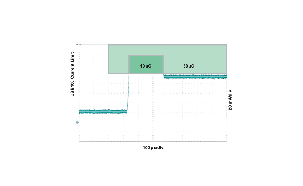
The bq24079QW-Q1 is USB IF compliant for the inrush current testing. The USB spec allows up to 10 μF to be hard started, which establishes 50 μC as the maximum inrush charge value when exceeding 100 mA. The input current limit for the bq24079QW-Q1 prevents the input current from exceeding this limit, even with system capacitances greater than 10 μF. Note that the input capacitance to the device must be selected small enough to prevent a violation (<10 μF), as this current is not limited. Figure 20 demonstrates the startup of the bq24079QW-Q1 and compares it to the USB-IF specification.
 Figure 20. USB-IF Inrush Current Test
 The input current limit selection is controlled by the state of the EN1 and EN2 pins. When using the resistor-programmable current limit, the input current limit is set by the value of the resistor connected from the ILIM pin to VSS, and is given by the equation:
The input current limit is adjustable up to 1.5 A. The valid resistor range is 1.1 kΩ to 8 kΩ.
When the IN source is connected, priority is given to the system load. The DPPM and Battery Supplement modes are used to maintain the system load. These modes are explained in detail in the following sections.