SLUSCM2B October   2017  – November 2018

PRODUCTION DATA.  

  1. Features
  2. Applications
  3. Description
    1.     Typical Application Circuit
  4. Revision History
  5. Description (continued)
  6. Device Comparison Table
  7. Pin Configuration and Functions
    1.     Pin Functions
  8. Specifications
    1. 8.1 Absolute Maximum Ratings
    2. 8.2 ESD Ratings
    3. 8.3 Recommended Operating Conditions
    4. 8.4 Thermal Information
    5. 8.5 Electrical Characteristics
    6. 8.6 Typical Characteristics
  9. Detailed Description
    1. 9.1 Overview
    2. 9.2 Functional Block Diagram
    3. 9.3 Feature Description
      1. 9.3.1 Undervoltage Lockout (UVLO)
      2. 9.3.2 Power On
      3. 9.3.3 Overvoltage Protection (OVP)
      4. 9.3.4 Dynamic Power-path Management
        1. 9.3.4.1 Input Source Connected (Adapter or USB)
          1. 9.3.4.1.1 Input DPM Mode (VIN-DPM)
          2. 9.3.4.1.2 DPPM Mode
          3. 9.3.4.1.3 Battery Supplement Mode
        2. 9.3.4.2 Input Source Not Connected
      5. 9.3.5 Battery Charging
        1. 9.3.5.1 Charge Current Translator
        2. 9.3.5.2 Battery Detection And Recharge
        3. 9.3.5.3 Battery Disconnect (SYSOFF Input)
        4. 9.3.5.4 Dynamic Charge Timers (TMR Input)
        5. 9.3.5.5 Status Indicators (PGOOD, CHG)
        6. 9.3.5.6 Thermal Regulation And Thermal Shutdown
      6. 9.3.6 Battery Pack Temperature Monitoring
      7. 9.3.7 Half-Wave Adaptors
    4. 9.4 Device Functional Modes
      1. 9.4.1 Sleep Mode
  10. 10Application and Implementation
    1. 10.1 Application Information
    2. 10.2 Typical Application – bq24079QW-Q1 Charger Design Example
      1. 10.2.1 Design Requirements
      2. 10.2.2 Detailed Design Procedure
        1. 10.2.2.1 Calculations
          1. 10.2.2.1.1 Program the Fast Charge Current (ISET):
          2. 10.2.2.1.2 Program the Input Current Limit (ILIM)
          3. 10.2.2.1.3 Program 6.25-hour Fast-Charge Safety Timer (TMR)
        2. 10.2.2.2 TS Function
        3. 10.2.2.3 CHG and PGOOD
        4. 10.2.2.4 System ON/OFF (SYSOFF)
        5. 10.2.2.5 Selecting In, Out And Bat Pin Capacitors
      3. 10.2.3 Application Curves
  11. 11Power Supply Recommendations
  12. 12Layout
    1. 12.1 Layout Guidelines
    2. 12.2 Layout Example
    3. 12.3 Thermal Package
  13. 13Device and Documentation Support
    1. 13.1 Device Support
      1. 13.1.1 Third-Party Products Disclaimer
    2. 13.2 Documentation Support
      1. 13.2.1 Related Documentation
    3. 13.3 Receiving Notification of Documentation Updates
    4. 13.4 Community Resources
    5. 13.5 Trademarks
    6. 13.6 Electrostatic Discharge Caution
    7. 13.7 Glossary
  14. 14Mechanical, Packaging, and Orderable Information

Package Options

Refer to the PDF data sheet for device specific package drawings

Mechanical Data (Package|Pins)
  • RGT|16
Thermal pad, mechanical data (Package|Pins)
Orderable Information

Input DPM Mode (VIN-DPM)

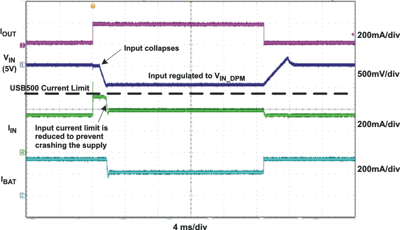
The bq24079QW-Q1 uses the VIN-DPM mode for operation from current-limited USB ports. When EN1 and EN2 are configured for USB100 (EN2 = 0, EN1 = 0) or USB500 (EN2 = 0, EN2 = 1) modes, the input voltage is monitored. If VIN falls to VIN-DPM, the input current limit is reduced to prevent the input voltage from falling further. This prevents the bq24079QW-Q1 from crashing poorly designed or incorrectly configured USB sources. Figure 21 shows the VIN-DPM behavior to a current limited source. In this figure, the input source has a 400-mA current limit and the device is in USB500 mode (EN1 = 1, EN2 = 0).
bq24079QW-Q1 dpm_wave_lus810.gifFigure 21. VIN-DPM Waveform