SLUSCM2B October 2017 – November 2018
PRODUCTION DATA.
- 1 Features
- 2 Applications
- 3 Description
- 4 Revision History
- 5 Description (continued)
- 6 Device Comparison Table
- 7 Pin Configuration and Functions
- 8 Specifications
-
9 Detailed Description
- 9.1 Overview
- 9.2 Functional Block Diagram
- 9.3 Feature Description
- 9.4 Device Functional Modes
-
10Application and Implementation
- 10.1 Application Information
- 10.2 Typical Application – bq24079QW-Q1 Charger Design Example
- 11Power Supply Recommendations
- 12Layout
- 13Device and Documentation Support
- 14Mechanical, Packaging, and Orderable Information
Package Options
Refer to the PDF data sheet for device specific package drawings
Mechanical Data (Package|Pins)
- RGT|16
Thermal pad, mechanical data (Package|Pins)
- RGT|16
Orderable Information
8.5 Electrical Characteristics
Over ambient temperature range (–40°C ≤ TA ≤ 125°C) and the recommended supply voltage range (unless otherwise noted)| PARAMETER | TEST CONDITIONS | MIN | TYP | MAX | UNIT | ||
|---|---|---|---|---|---|---|---|
| INPUT | |||||||
| UVLO | Undervoltage lock-out | VIN: 0 V → 4 V | 3.2 | 3.3 | 3.4 | V | |
| Vhys | Hysteresis on UVLO | VIN: 4 V → 0 V | 200 | 300 | mV | ||
| VIN(DT) | Input power detection threshold | Input power detected when VIN > VBAT + VIN(DT)
VBAT = 3.6 V, VIN: 3.5 V → 4 V |
50 | 80 | 135 | mV | |
| Vhys | Hysteresis on VIN(DT) | VBAT = 3.6 V, VIN: 4 V → 3.5 V | 20 | mV | |||
| tDGL(PGOOD) | Deglitch time, input power detected status | Time measured from VIN: 0 V → 5 V with 1-μs
rise time to PGOOD = LO |
1.2 | ms | |||
| VOVP | Input overvoltage protection threshold | VIN: 5 V → 7 V | 6.4 | 6.6 | 6.8 | V | |
| Vhys | Hysteresis on OVP | VIN: 7 V → 5V | 110 | mV | |||
| tDGL(OVP) | Input overvoltage blanking time (OVP fault deglitch) | 50 | μs | ||||
| tREC | Input overvoltage recovery time | Time measured from VIN: 11 V → 5 V with 1-μs
fall time to PGOOD = LO |
1.2 | ms | |||
| ILIM, ISET SHORT CIRCUIT DETECTION (CHECKED DURING STARTUP) | |||||||
| ISC | Current source | VIN > UVLO and VIN > VBAT + VIN(DT) | 1.3 | mA | |||
| VSC | VIN > UVLO and VIN > VBAT + VIN(DT) | 520 | mV | ||||
| QUIESCENT CURRENT | |||||||
| IBAT(PDWN) | Sleep current into BAT pin | CE = LO or HI, Input power not detected,
No load on OUT pin, TA ≤ 125°C |
4.4 | 13 | μA | ||
| IIN | Standby current into IN pin | EN1 = HI, EN2 = HI, VIN = 6 V, TA ≤ 125°C | 38.8 | 55 | μA | ||
| EN1 = HI, EN2 = HI, VIN = 10 V, TA ≤ 125°C | 90.2 | 200 | |||||
| ICC | Active supply current, IN pin | CE = LO, VIN = 6 V, No load on OUT pin,
VBAT > VBAT(REG), (EN1, EN2) ≠ (HI, HI) |
1.5 | mA | |||
| POWER PATH | |||||||
| VDO(IN-OUT) | VIN – VOUT | VIN = 4.3 V, IIN = 1 A, VBAT = 4.1 V | 300 | 475 | mV | ||
| VDO(BAT-OUT) | VBAT – VOUT | IOUT = 1 A, VIN = 0 V, VBAT > 3 V | 50 | 100 | mV | ||
| VO(REG) | OUT pin voltage regulation | VIN > VOUT + VDO(IN-OUT) | 5.4 | 5.5 | 5.65 | V | |
| IINmax | Maximum input current | EN1 = LO, EN2 = LO | 90 | 95 | 101 | mA | |
| EN1 = HI, EN2 = LO | 440 | 475 | 500 | ||||
| EN2 = HI, EN1 = LO | KILIM/RILIM | A | |||||
| KILIM | Maximum input current factor | ILIM = 500 mA to 1.5 A | 1500 | 1610 | 1720 | AΩ | |
| ILIM = 200 mA to 500 mA | 1300 | 1525 | 1770 | ||||
| IINmax | Programmable input current limit range | EN2 = HI, EN1 = LO, RILIM = 8 kΩ to 1.1 kΩ | 200 | 1500 | mA | ||
| VIN-DPM | Input voltage threshold when input current is reduced | EN2 = LO, EN1 = X | 4.35 | 4.5 | 4.63 | V | |
| VDPPM | Output voltage threshold when charging current is reduced | 4.2 | 4.3 | 4.4 | V | ||
| VBSUP1 | Enter battery supplement mode | VBAT = 3.6 V, RILIM = 1.5 kΩ, RLOAD = 10 Ω → 2 Ω | VOUT ≤ VBAT –40mV | V | |||
| VBSUP2 | Exit battery supplement mode | VBAT = 3.6 V, RILIM = 1.5 kΩ, RLOAD = 2 Ω → 10 Ω | VOUT ≥ VBAT–20mV | V | |||
| VO(SC1) | Output short-circuit detection threshold, power-on | VIN > VUVLO and VIN > VBAT + VIN(DT) | 0.8 | 0.9 | 1 | V | |
| VO(SC2) | Output short-circuit detection threshold, supplement mode VBAT – VOUT > VO(SC2) indicates short-circuit | VIN > VUVLO and VIN > VBAT + VIN(DT) | 200 | 250 | 300 | mV | |
| tDGL(SC2) | Deglitch time, supplement mode short circuit | 250 | μs | ||||
| tREC(SC2) | Recovery time, supplement mode short circuit | 60 | ms | ||||
| BATTERY CHARGER | |||||||
| IBAT | Source current for BAT pin short-circuit detection | VBAT = 1.5 V | 4 | 7.5 | 11 | mA | |
| VBAT(SC) | BAT pin short-circuit detection threshold | VBAT rising | 1.6 | 1.8 | 2 | V | |
| VBAT(REG) | Battery charge voltage | 4.059 | 4.100 | 4.141 | V | ||
| VLOWV | Pre-charge to fast-charge transition threshold | VIN > VUVLO and VIN > VBAT + VIN(DT) | 2.9 | 3 | 3.1 | V | |
| tDGL1(LOWV) | Deglitch time on pre-charge to fast-charge transition | 25 | ms | ||||
| tDGL2(LOWV) | Deglitch time on fast-charge to pre-charge transition | 25 | ms | ||||
| ICHG | Battery fast charge current range | VBAT(REG) > VBAT > VLOWV, VIN = 5 V, CE = LO,
EN1 = LO, EN2 = HI |
100 | 1500 | mA | ||
| Battery fast charge current | CE = LO, EN1= LO, EN2 = HI,
VBAT > VLOWV, VIN = 5 V, IINmax > ICHG, No load on OUT pin, Thermal loop and DPPM loop not active |
KISET/RISET | A | ||||
| KISET | Fast charge current factor | 797 | 890 | 975 | AΩ | ||
| IPRECHG | Pre-charge current | KPRECHG/RISET | A | ||||
| KPRECHG | Pre-charge current factor | 55 | 88 | 118 | AΩ | ||
| ITERM | Termination comparator detection threshold (internally set) | CE = LO, (EN1, EN2) ≠ (LO, LO),
VBAT > VRCH, t < tMAXCH, VIN = 5 V, DPPM loop and thermal loop not active |
0.09×ICHG | 0.1×ICHG | 0.11×ICHG | A | |
| CE = LO, (EN1, EN2) = (LO, LO),
VBAT > VRCH, t < tMAXCH, VIN = 5 V, DPPM loop and thermal loop not active |
0.027×ICHG | 0.033×ICHG | 0.040×ICHG | ||||
| tDGL(TERM) | Deglitch time, termination detected | 25 | ms | ||||
| VRCH | Recharge detection threshold | VIN > VUVLO and VIN > VBAT + VIN(DT) | 50 | 100 | 145 | mV | |
| tDGL(RCH) | Deglitch time, recharge threshold detected | 62.5 | ms | ||||
| tDGL(NO-IN) | Delay time, input power loss to OUT LDO turn-off | VBAT = 3.6 V. Time measured from
VIN: 5 V → 3 V, 1-μs fall time |
20 | ms | |||
| IBAT(DET) | Sink current for battery detection | VBAT = 2.5 V | 5 | 7.5 | 10 | mA | |
| tDET | Battery detection timer | BAT high or low | 250 | ms | |||
| BATTERY CHARGING TIMERS | |||||||
| tPRECHG | Pre-charge safety timer value | TMR = floating | 1440 | 1800 | 2160 | s | |
| tMAXCHG | Charge safety timer value | TMR = floating | 14400 | 18000 | 21600 | s | |
| tPRECHG | Pre-charge safety timer value | 18 kΩ < RTMR < 72 kΩ | RTMR × KTMR | s | |||
| tMAXCHG | Charge safety timer value | 18 kΩ < RTMR < 72 kΩ | 10×R TMR ×KTMR | s | |||
| KTMR | Timer factor | 36 | 48 | 60 | s/kΩ | ||
| BATTERY-PACK NTC MONITOR(1) | |||||||
| INTC | NTC bias current | VIN > UVLO and VIN > VBAT + VIN(DT) | 71 | 75 | 80 | μA | |
| VHOT | High temperature trip point | Battery charging, VTS Falling | 270 | 300 | 330 | mV | |
| VHYS(HOT) | Hysteresis on high trip point | Battery charging, VTS Rising from VHOT | 30 | mV | |||
| VCOLD | Low temperature trip point | Battery charging, VTS Rising | 2000 | 2100 | 2200 | mV | |
| VHYS(COLD) | Hysteresis on low trip point | Battery charging, VTS Falling from VCOLD | 300 | mV | |||
| tDGL(TS) | Deglitch time, pack temperature fault detection | TS fault detected to charger disable | 50 | ms | |||
| THERMAL REGULATION | |||||||
| TJ(REG) | Temperature regulation limit | 125 | °C | ||||
| TJ(OFF) | Thermal shutdown temperature | TJ Rising | 155 | °C | |||
| TJ(OFF-HYS) | Thermal shutdown hysteresis | 20 | °C | ||||
| LOGIC LEVELS ON EN1, EN2, CE, SYSOFF | |||||||
| VIL | Logic LOW input voltage | 0 | 0.4 | V | |||
| VIH | Logic HIGH input voltage | 1.4 | 6 | V | |||
| IIL | Input sink current | VIL= 0 V | 1 | μA | |||
| IIH | Input source current | VIH= 1.4 V | 10 | μA | |||
| LOGIC LEVELS ON PGOOD, CHG | |||||||
| VOL | Output LOW voltage | ISINK = 5 mA | 0.4 | V | |||
(1) These numbers set trip points of 0°C and 50°C while charging, with 3°C hysteresis on the trip points, with a Vishay Type 2 curve NTC with an R25 of 10 kΩ.
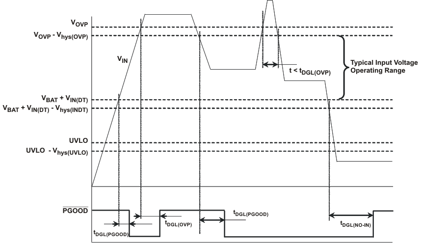
 Figure 1. Power-Up, Power-Down, Power Good Indication
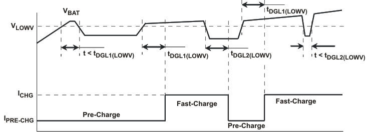
  Figure 2. Pre- to Fast-Charge, Fast- to Pre-Charge Transition – tDGL1(LOWV), tDGL2(LOWV)
  Figure 3. Recharge – tDGL(RCH)
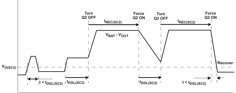
  Figure 4. OUT Short-Circuit – Supplement Mode
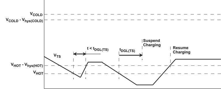
  Figure 5. Battery Pack Temperature Sensing – TS Pin. Battery Temperature Increasing