SBOS948F February 2019 – May 2021 BUF634A
PRODUCTION DATA
- 1 Features
- 2 Applications
- 3 Description
- 4 Revision History
- 5 Device Comparison Table
- 6 Pin Configuration and Functions
- 7 Specifications
- 8 Detailed Description
- 9 Application and Implementation
- 10Power Supply Recommendations
- 11Layout
- 12Device and Documentation Support
- 13Mechanical, Packaging, and Orderable Information
Package Options
Refer to the PDF data sheet for device specific package drawings
Mechanical Data (Package|Pins)
- D|8
- DDA|8
- DRB|8
Thermal pad, mechanical data (Package|Pins)
Orderable Information
9.1.1 High-Frequency Applications
The excellent bandwidth and fast slew rate of the BUF634A are useful in a variety of high-frequency, open-loop applications. When operated in an open-loop application, printed circuit board (PCB) layout and bypassing techniques can affect dynamic performance. Figure 9-2 through Figure 9-6 illustrate various application circuit examples for the BUF634A.
For best results, use a ground-plane-type circuit board layout and bypass the power supplies with 0.1-µF ceramic chip capacitors at the device pins in parallel with solid tantalum 10-µF capacitors. Source resistance affects high-frequency peaking, step-response overshoot, and ringing. Best response is usually achieved with a series input resistor of 25 Ω to 200 Ω, depending on the signal source. Response with some loads (especially capacitive) can be improved with a resistor of 10 Ω to 150 Ω in series with the output. When driving multiple device under test (DUT) inputs in automatic test equipment (ATE) testers (large capacitive load), as illustrated in Figure 9-3, place an isolation resistor at the output of the BUF634A for adequate phase margin and stability.
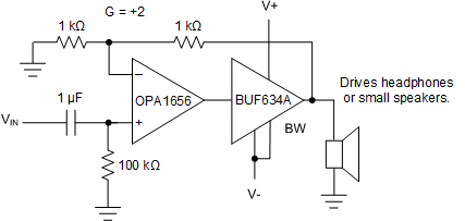 Figure 9-2 High-Performance Headphone Driver
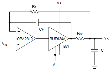 Figure 9-3 ATE and Test Pin Driver
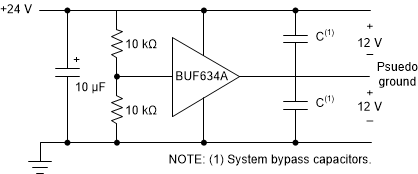 Figure 9-4 Pseudo-Ground Driver
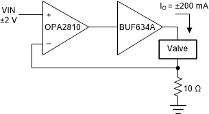 Figure 9-5 Current-Output Valve Driver
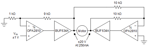 Figure 9-6 Bridge-Connected Motor Driver