SNLS647I December   2019  – August 2025 DP83826E , DP83826I

PRODUCTION DATA  

  1.   1
  2. Features
  3. Applications
  4. Description
  5. Mode Comparison Tables
  6. Pin Configuration and Functions (ENHANCED Mode)
  7. Pin Configuration and Functions (BASIC Mode)
  8. Specifications
    1. 7.1 Absolute Maximum Ratings
    2. 7.2 ESD Ratings
    3. 7.3 Recommended Operating Conditions
    4. 7.4 Thermal Information
    5. 7.5 Electrical Characteristics
    6. 7.6 Timing Requirements
    7. 7.7 Timing Diagrams
    8. 7.8 Typical Characteristics
  9. Detailed Description
    1. 8.1 Overview
    2. 8.2 Functional Block Diagram
    3. 8.3 Feature Description
      1. 8.3.1  Auto-Negotiation (Speed/Duplex Selection)
      2. 8.3.2  Auto-MDIX Resolution
      3. 8.3.3  Energy Efficient Ethernet
        1. 8.3.3.1 EEE Overview
        2. 8.3.3.2 EEE Negotiation
      4. 8.3.4  EEE for Legacy MACs Not Supporting 802.3az
      5. 8.3.5  Wake-on-LAN Packet Detection
        1. 8.3.5.1 Magic Packet Structure
        2. 8.3.5.2 Magic Packet Example
        3. 8.3.5.3 Wake-on-LAN Configuration and Status
      6. 8.3.6  Low Power Modes
        1. 8.3.6.1 Active Sleep
        2. 8.3.6.2 IEEE Power-Down
        3. 8.3.6.3 Deep Power Down State
      7. 8.3.7  RMII Repeater Mode
      8. 8.3.8  Clock Output
      9. 8.3.9  Media Independent Interface (MII)
      10. 8.3.10 Reduced Media Independent Interface (RMII)
      11. 8.3.11 Serial Management Interface
        1. 8.3.11.1 Extended Register Space Access
        2. 8.3.11.2 Write Address Operation
        3. 8.3.11.3 Read Address Operation
        4. 8.3.11.4 Write (No Post Increment) Operation
        5. 8.3.11.5 Read (No Post Increment) Operation
        6. 8.3.11.6 Example Write Operation (No Post Increment)
      12. 8.3.12 100BASE-TX
        1. 8.3.12.1 100BASE-TX Transmitter
          1. 8.3.12.1.1 Code-Group Encoding and Injection
          2. 8.3.12.1.2 Scrambler
          3. 8.3.12.1.3 NRZ to NRZI Encoder
          4. 8.3.12.1.4 Binary to MLT-3 Converter
        2. 8.3.12.2 100BASE-TX Receiver
      13. 8.3.13 10BASE-Te
        1. 8.3.13.1 Squelch
        2. 8.3.13.2 Normal Link Pulse Detection and Generation
        3. 8.3.13.3 Jabber
        4. 8.3.13.4 Active Link Polarity Detection and Correction
      14. 8.3.14 Loopback Modes
        1. 8.3.14.1 Near-end Loopback
        2. 8.3.14.2 MII Loopback
        3. 8.3.14.3 PCS Loopback
        4. 8.3.14.4 Digital Loopback
        5. 8.3.14.5 Analog Loopback
        6. 8.3.14.6 Far-End (Reverse) Loopback
      15. 8.3.15 BIST Configurations
      16. 8.3.16 Cable Diagnostics
        1. 8.3.16.1 Time Domain Reflectometry (TDR)
      17. 8.3.17 Fast Link-Drop Functionality
      18. 8.3.18 LED and GPIO Configuration
    4. 8.4 Programming
      1. 8.4.1 Hardware Bootstraps Configuration
        1. 8.4.1.1 Bootstrap Configurations (ENHANCED Mode)
        2. 8.4.1.2 Strap Configuration (BASIC Mode)
    5. 8.5 Register Maps
      1. 8.5.1 DP83826 Registers
  10. Application and Implementation
    1. 9.1 Application Information
    2. 9.2 Typical Applications
      1. 9.2.1 Twisted-Pair Interface (TPI) Network Circuit
      2. 9.2.2 Transformer Recommendations
      3. 9.2.3 Capacitive DC Blocking
      4. 9.2.4 Design Requirements
        1. 9.2.4.1 Clock Requirements
          1. 9.2.4.1.1 Oscillator
          2. 9.2.4.1.2 Crystal
      5. 9.2.5 Detailed Design Procedure
        1. 9.2.5.1 MII Layout Guidelines
        2. 9.2.5.2 RMII Layout Guidelines
        3. 9.2.5.3 MDI Layout Guidelines
      6. 9.2.6 Application Curves
    3. 9.3 Power Supply Recommendations
    4. 9.4 Layout
      1. 9.4.1 Layout Guidelines
        1. 9.4.1.1 Signal Traces
        2. 9.4.1.2 Return Path
        3. 9.4.1.3 Transformer Layout
        4. 9.4.1.4 Metal Pour
        5. 9.4.1.5 PCB Layer Stacking
          1. 9.4.1.5.1 Layout Example
  11. 10Device and Documentation Support
    1. 10.1 Related Documentation
    2. 10.2 Receiving Notification of Documentation Updates
    3. 10.3 Support Resources
    4. 10.4 Trademarks
    5. 10.5 Electrostatic Discharge Caution
    6. 10.6 Glossary
  12. 11Revision History
  13. 12Mechanical, Packaging, and Orderable Information

Package Options

Mechanical Data (Package|Pins)
Thermal pad, mechanical data (Package|Pins)
Orderable Information
Crystal

The use of a 25MHz, parallel resonant, 20pF load crystal is recommended if operating with a crystal. See Figure 9-4 for a typical connection diagram for a crystal resonator circuit. The load capacitor values vary with the crystal vendors; check with the vendor for the recommended loads. Refer to the application report Selection and specification of crystals for Texas Instruments ethernet physical layer transceivers for more details.
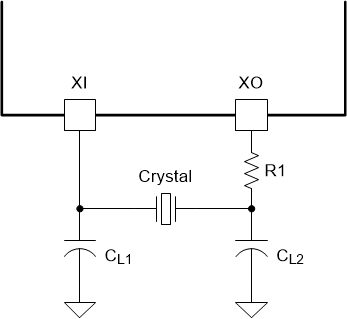
DP83826E DP83826I Crystal Oscillator CircuitFigure 9-4 Crystal Oscillator Circuit
Table 9-2 25MHz Crystal Specification
PARAMETERTEST CONDITIONSMINTYPMAXUNIT
Frequency25MHz
Frequency toleranceIncluding operational temperature, aging and other factors–5050ppm
Load capacitance1540pF
ESR50Ω