SLOS916B June   2016  – June 2020 DRV2511-Q1

PRODUCTION DATA.  

  1. Features
  2. Applications
  3. Description
    1.     Simplified Schematic
  4. Revision History
  5. Pin Configuration and Functions
    1.     Pin Functions
  6. Specifications
    1. 6.1 Absolute Maximum Ratings
    2. 6.2 ESD Ratings
    3. 6.3 Recommended Operating Conditions
    4. 6.4 Thermal Information
    5. 6.5 Electrical Characteristics
    6. 6.6 Switching Characteristics
    7. 6.7 Typical Characteristics
  7. Detailed Description
    1. 7.1 Overview
    2. 7.2 Functional Block Diagram
    3. 7.3 Feature Description
      1. 7.3.1 Analog Input and Configurable Pre-amplifier
      2. 7.3.2 Pulse-Width Modulator (PWM)
      3. 7.3.3 Designed for low EMI
      4. 7.3.4 Device Protection Systems
    4. 7.4 Device Functional Modes
      1. 7.4.1 Operation in Shutdown Mode
      2. 7.4.2 Operation in Standby Mode
      3. 7.4.3 Operation in Active Mode
  8. Programming
    1. 8.1 Gain
  9. Application and Implementation
    1. 9.1 Application Information
    2. 9.2 Typical Application, Single Ended Input
      1. 9.2.1 Design Requirements
      2. 9.2.2 Detailed Design Procedure
        1. 9.2.2.1 Optional Components
        2. 9.2.2.2 Capacitor Selection
        3. 9.2.2.3 Solenoid Selection
        4. 9.2.2.4 Output Filter Considerations
      3. 9.2.3 Application Curves
      4. 9.2.4 Typical Application, Differential Input
  10. 10Power Supply Recommendations
    1. 10.1 Power Dissipation and Maximum Ambient Temperature
  11. 11Layout
    1. 11.1 Layout Guidelines
    2. 11.2 Layout Example
  12. 12Device and Documentation Support
    1. 12.1 Documentation Support
    2. 12.2 Receiving Notification of Documentation Updates
    3. 12.3 Community Resources
    4. 12.4 Trademarks
    5. 12.5 Electrostatic Discharge Caution
    6. 12.6 Glossary
  13. 13Mechanical, Packaging, and Orderable Information

Package Options

Mechanical Data (Package|Pins)
Thermal pad, mechanical data (Package|Pins)
Orderable Information

Analog Input and Configurable Pre-amplifier

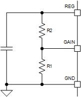
The DRV2511-Q1 device features a differential input stage that cancels common-mode noise that appears on the inputs. The DRV2511-Q1 device also features four gain settings that are configurable via external resistors.

Table 1. Gain Configuration Table

GAIN R1 R2 INPUT IMPEDANCE
20 dB 5.6 kΩ open 60 kΩ
26 dB 20 kΩ 100 kΩ 30 kΩ
32 dB 39 kΩ 100 kΩ 15 kΩ
36 dB 47 kΩ 75 kΩ 9 kΩ
DRV2511-Q1 gain_confit_sch_slos916.gifFigure 3. Gain Configuration