SLOS916B June   2016  – June 2020 DRV2511-Q1

PRODUCTION DATA.  

  1. Features
  2. Applications
  3. Description
    1.     Simplified Schematic
  4. Revision History
  5. Pin Configuration and Functions
    1.     Pin Functions
  6. Specifications
    1. 6.1 Absolute Maximum Ratings
    2. 6.2 ESD Ratings
    3. 6.3 Recommended Operating Conditions
    4. 6.4 Thermal Information
    5. 6.5 Electrical Characteristics
    6. 6.6 Switching Characteristics
    7. 6.7 Typical Characteristics
  7. Detailed Description
    1. 7.1 Overview
    2. 7.2 Functional Block Diagram
    3. 7.3 Feature Description
      1. 7.3.1 Analog Input and Configurable Pre-amplifier
      2. 7.3.2 Pulse-Width Modulator (PWM)
      3. 7.3.3 Designed for low EMI
      4. 7.3.4 Device Protection Systems
    4. 7.4 Device Functional Modes
      1. 7.4.1 Operation in Shutdown Mode
      2. 7.4.2 Operation in Standby Mode
      3. 7.4.3 Operation in Active Mode
  8. Programming
    1. 8.1 Gain
  9. Application and Implementation
    1. 9.1 Application Information
    2. 9.2 Typical Application, Single Ended Input
      1. 9.2.1 Design Requirements
      2. 9.2.2 Detailed Design Procedure
        1. 9.2.2.1 Optional Components
        2. 9.2.2.2 Capacitor Selection
        3. 9.2.2.3 Solenoid Selection
        4. 9.2.2.4 Output Filter Considerations
      3. 9.2.3 Application Curves
      4. 9.2.4 Typical Application, Differential Input
  10. 10Power Supply Recommendations
    1. 10.1 Power Dissipation and Maximum Ambient Temperature
  11. 11Layout
    1. 11.1 Layout Guidelines
    2. 11.2 Layout Example
  12. 12Device and Documentation Support
    1. 12.1 Documentation Support
    2. 12.2 Receiving Notification of Documentation Updates
    3. 12.3 Community Resources
    4. 12.4 Trademarks
    5. 12.5 Electrostatic Discharge Caution
    6. 12.6 Glossary
  13. 13Mechanical, Packaging, and Orderable Information

Package Options

Mechanical Data (Package|Pins)
Thermal pad, mechanical data (Package|Pins)
Orderable Information

Typical Application, Single Ended Input

To use the DRV2511-Q1 with a single-ended source, apply either a voltage divider to bias INB to 3 V, tie to GND or use a 0.1-μF cap from INB to GND to have the device self bias. Apply the single-ended signal to the INA pin.
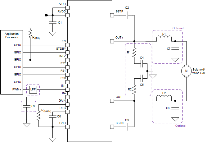
DRV2511-Q1 app_sch_SE_slos916.gifFigure 5. Typical Application Schematic