SLOS751E March   2013  – January 2023 DRV2667

PRODUCTION DATA  

  1. Features
  2. Applications
  3. Description
  4. Revision History
  5. Pin Configuration and Functions
  6. Specifications
    1. 6.1 Absolute Maximum Ratings
    2. 6.2 ESD Ratings
    3. 6.3 Recommended Operating Conditions
    4. 6.4 Thermal Information
    5. 6.5 Electrical Characteristics
    6. 6.6 Timing Requirements
    7. 6.7 Switching Characteristics
    8. 6.8 Typical Characteristics
  7. Detailed Description
    1. 7.1 Overview
    2. 7.2 Functional Block Diagram
    3. 7.3 Feature Description
      1. 7.3.1  Support for Haptic Piezo Actuators
      2. 7.3.2  Flexible Front End Interface
      3. 7.3.3  Ramp Down Behavior
      4. 7.3.4  Low Latency Startup
      5. 7.3.5  Low Power Standby Mode
      6. 7.3.6  Device Reset
      7. 7.3.7  Amplifier Gain
      8. 7.3.8  Adjustable Boost Voltage
      9. 7.3.9  Adjustable Current Limit
      10. 7.3.10 Internal Charge Pump
      11. 7.3.11 Device Protection
        1. 7.3.11.1 Thermal Protection
        2. 7.3.11.2 Overcurrent Protection
        3. 7.3.11.3 Brownout Protection
    4. 7.4 Device Functional Modes
      1. 7.4.1 FIFO Mode
        1. 7.4.1.1 Waveform Timeout
      2. 7.4.2 Direct Playback from RAM Mode
      3. 7.4.3 Waveform Synthesis Playback Mode
      4. 7.4.4 Waveform Sequencer
      5. 7.4.5 Analog Playback Mode
      6. 7.4.6 Low Voltage Operation Mode
    5. 7.5 Programming
      1. 7.5.1 Programming the Boost Voltage
      2. 7.5.2 Programming the Boost Current Limit
      3. 7.5.3 Programming the RAM
        1. 7.5.3.1 Accessing the RAM
        2. 7.5.3.2 RAM Format
          1. 7.5.3.2.1 Programming the Waveform Sequencer
      4. 7.5.4 I2C Interface
        1. 7.5.4.1 General I2C Operation
        2. 7.5.4.2 Single-Byte and Multiple-Byte Transfers
        3. 7.5.4.3 Single-Byte Write
        4. 7.5.4.4 Multiple-Byte Write and Incremental Multiple-Byte Write
        5. 7.5.4.5 Single-Byte Read
        6. 7.5.4.6 Multiple-Byte Read
    6. 7.6 Register Map
      1. 7.6.1  Address: 0x00
      2. 7.6.2  Address: 0x01
      3. 7.6.3  Address: 0x02
      4. 7.6.4  Address: 0x03
      5. 7.6.5  Address: 0x04
      6. 7.6.6  Address: 0x05
      7. 7.6.7  Address: 0x06
      8. 7.6.8  Address: 0x07
      9. 7.6.9  Address: 0x08
      10. 7.6.10 Address: 0x09
      11. 7.6.11 Address: 0x0A
      12. 7.6.12 Address: 0x0B
      13. 7.6.13 Address: 0xFF
  8. Application and Implementation
    1. 8.1 Application Information
    2. 8.2 Typical Application
      1. 8.2.1 Design Requirements
      2. 8.2.2 Detailed Design Procedure
        1. 8.2.2.1 Inductor Selection
        2. 8.2.2.2 Piezo Actuator Selection
        3. 8.2.2.3 Boost Capacitor Selection
        4. 8.2.2.4 Bulk Capacitor Selection
      3. 8.2.3 Application Curves
    3. 8.3 Initialization Setup
      1. 8.3.1 Initialization Procedure
      2. 8.3.2 Typical Usage Examples
        1. 8.3.2.1 Single Click or Alert Example
        2. 8.3.2.2 Library Storage Example
  9. Power Supply Recommendations
  10. 10Layout
    1. 10.1 Layout Guidelines
    2. 10.2 Layout Example
  11. 11Device and Documentation Support
    1. 11.1 Receiving Notification of Documentation Updates
    2. 11.2 Community Resources
    3. 11.3 Trademarks
  12. 12Mechanical, Packaging, and Orderable Information

Package Options

Mechanical Data (Package|Pins)
Thermal pad, mechanical data (Package|Pins)
Orderable Information

Typical Characteristics

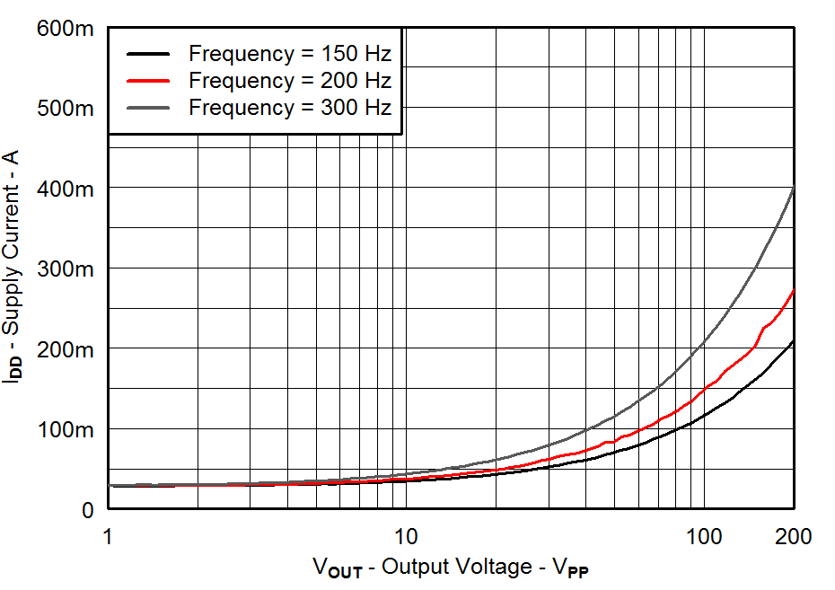
GUID-7A47FFE7-79FC-4601-A14E-1C235C8A5074-low.svg
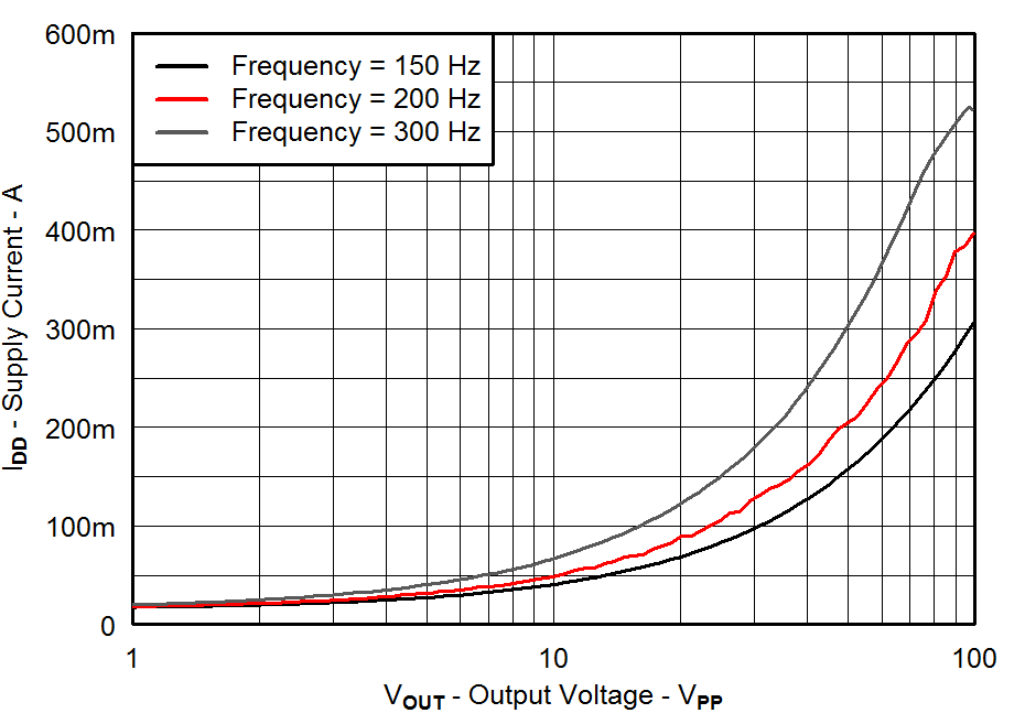
f = 200 HzPVDD = 105 V
CLOAD = 47 nFGain = 40 dB
Figure 6-3 Supply Current vs Output Voltage
GUID-B777A177-8E16-4828-B30F-9343FC2DFCB9-low.svg
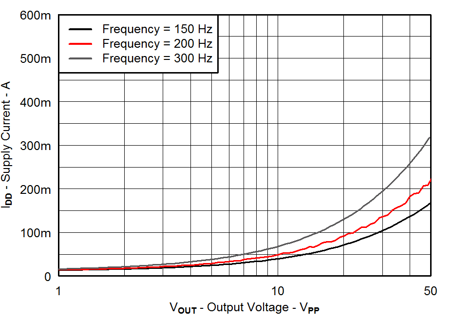
f = 200 HzPVDD = 55 V
CLOAD = 330 nFGain = 34 dB
Figure 6-5 Supply Current vs Output Voltage
GUID-C83B26D1-D6A3-4565-9794-DB836096AFC2-low.svg
f = 200 HzPVDD = 30 V
CLOAD = 680 nFGain = 28 dB
Figure 6-7 Supply Current vs Output Voltage
GUID-020221C6-0103-4391-97C8-49169F53C22A-low.svg
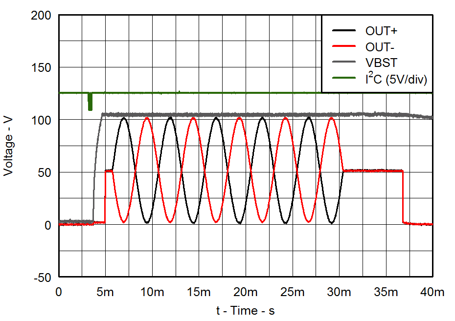
f = 200 HzPVDD = 105 V
CLOAD = 47 nFGain = 40 dB
Figure 6-9 Total Harmonic Distortion + Noise vs Output Voltage
GUID-42FAC146-F648-4ADF-8CB2-651F0A7231FF-low.svg
f = 200 HzPVDD = 55 V
CLOAD = 330 nFGain = 34 dB
Figure 6-11 Total Harmonic Distortion + Noise vs Output Voltage
GUID-5D0BC7EA-580A-4394-8BAC-5FF72E2B3F73-low.svg
f = 200 HzPVDD = 30 V
CLOAD = 680 nFGain = 28 dB
Figure 6-13 Total Harmonic Distortion + Noise vs Output Voltage
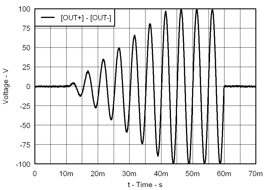
GUID-2CCF416A-EE82-4F6B-8169-A0A719616587-low.png
f = 200 HzPVDD = 105 V
CLOAD = 47 nFGain = 40 dB
Figure 6-15 Example Waveform – Envelope Up
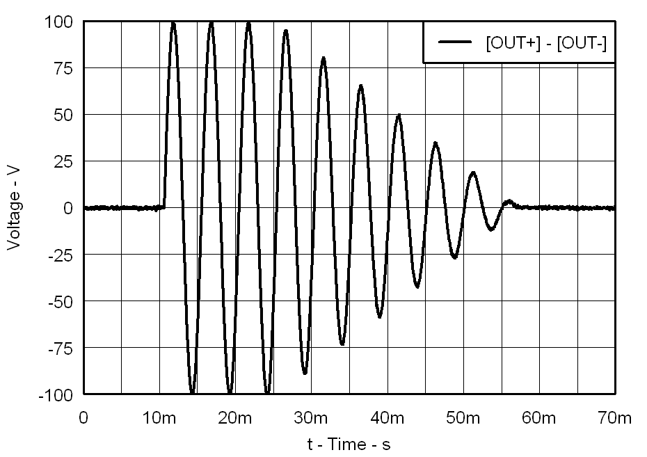
GUID-267FAB4B-1401-4AF1-8C28-D7AC9949BFC4-low.png
Figure 6-17 Example Waveform – Envelope Down
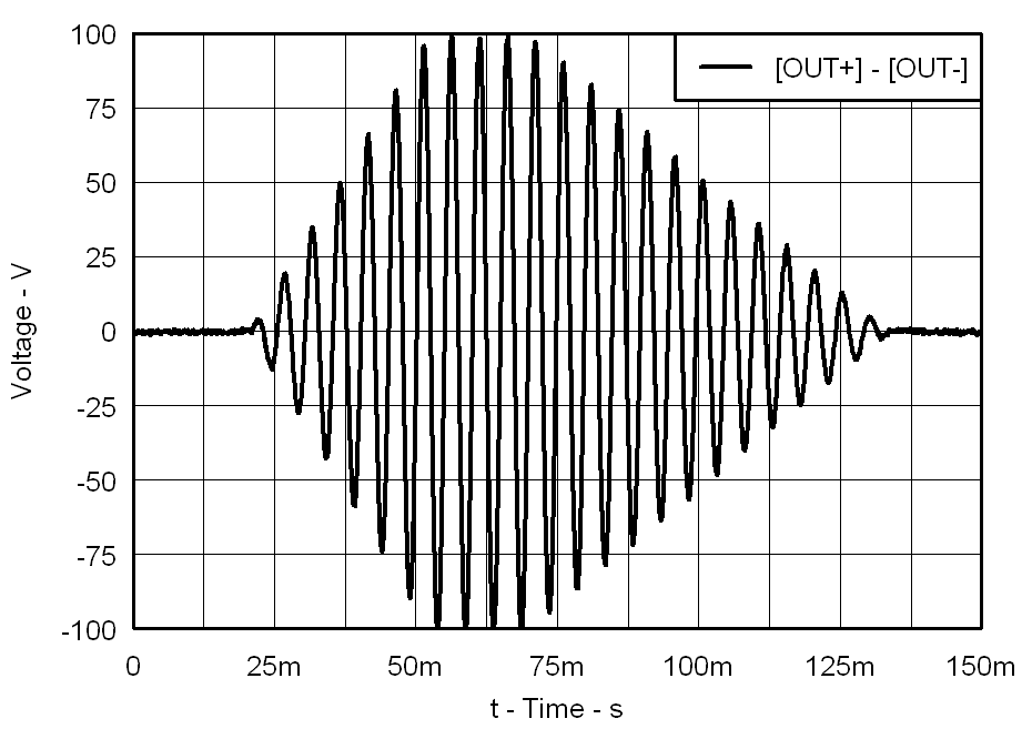
GUID-EA550FAF-6595-450D-91BD-4E35415D5D72-low.png
Figure 6-19 Example Waveform – Envelope Up and Down
GUID-77C7F243-E888-41AB-BD69-964B3C5B49FE-low.png
VDD = 3.6 VPVDD = 105 V
CLOAD = 47 nFGain = 40 dB
Figure 6-4 Supply Current vs Output Voltage
GUID-4AA22A10-C640-496D-B321-3117EF458726-low.png
VDD = 3.6 VPVDD = 55 V
CLOAD = 330 nFGain = 34 dB
Figure 6-6 Supply Current vs Output Voltage
GUID-9AB6A7F4-6892-4205-B47F-57EA6ACD57A3-low.png
VDD = 3.6 VPVDD = 30 V
CLOAD = 680 nFGain = 28 dB
Figure 6-8 Supply Current vs Output Voltage
GUID-3FC8613C-6638-47DA-8CB1-66B2BEE69B60-low.png
VDD = 3.6 VPVDD = 105 V
CLOAD = 47 nFGain = 40 dB
Figure 6-10 Typical Waveform
GUID-F6614739-0D55-4900-9312-F31C49D7F8AE-low.png
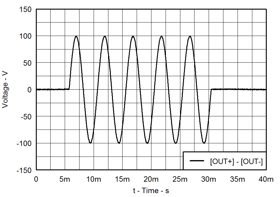
VDD = 3.6 VPVDD = 55 V
CLOAD = 330 nFGain = 34 dB
Figure 6-12 Typical Waveform - Differential
GUID-9A4DDC35-1F02-4CDA-917C-03192132FEB1-low.png
VDD = 3.6 VPVDD = 30 V
CLOAD = 680 nFGain = 28 dB
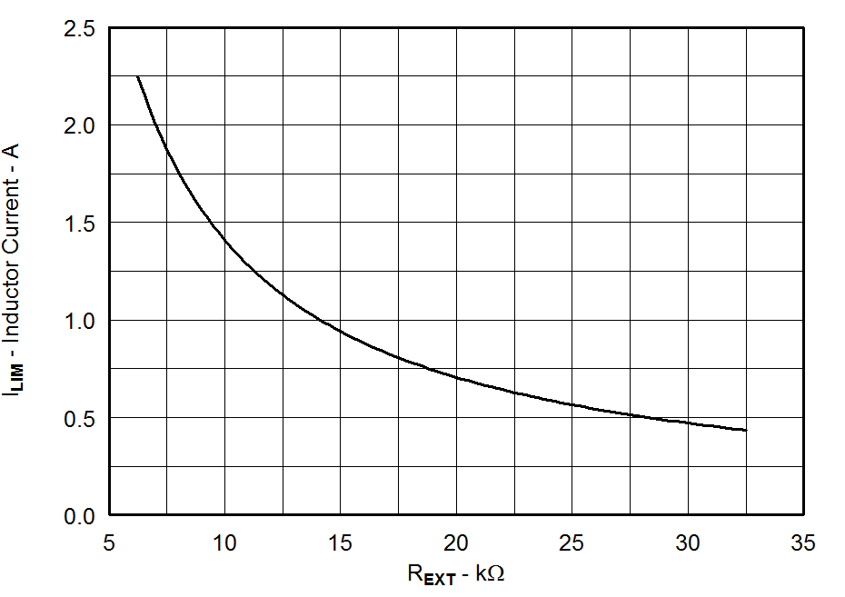
Figure 6-14 ILIM vs R(EXT)
GUID-A91F88DB-ECB1-42E9-90E8-D526ADF2050B-low.png
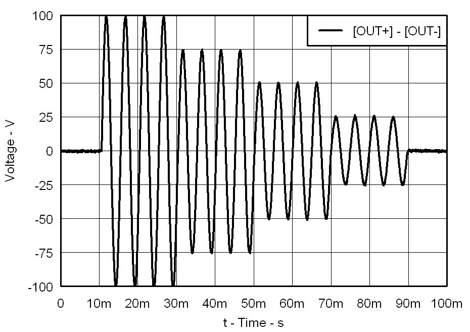
Figure 6-16 Example Waveform – Amplitude
GUID-485723D0-3C3A-4CD8-8E9F-DCB788877D68-low.png
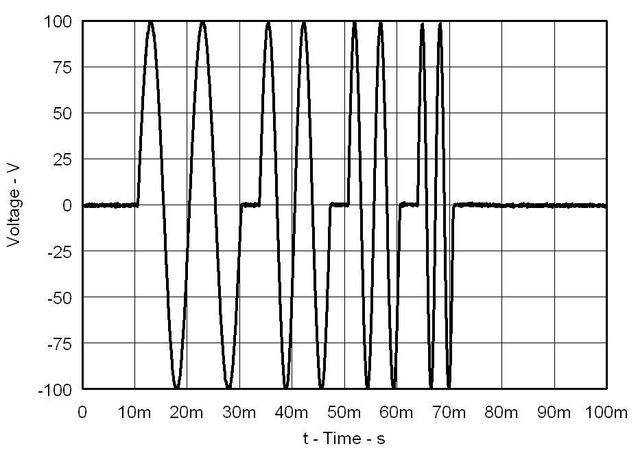
Figure 6-18 Example Waveform – Frequency
GUID-72D67534-673F-4DFE-A88A-D89E0B0AB941-low.png
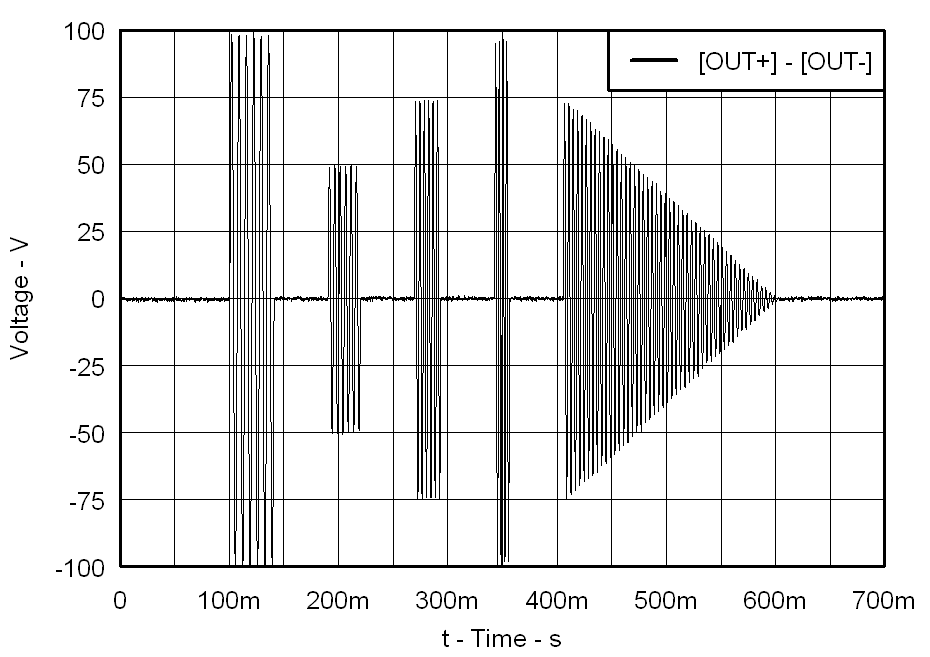
Figure 6-20 Example Waveform – Pinball Effect