SLVSFU5B February   2020  – August 2021 DRV8220

PRODUCTION DATA  

  1. Features
  2. Applications
  3. Description
  4. Revision History
  5. Device Comparison
  6. Pin Configuration and Functions
  7. Specifications
    1. 7.1 Absolute Maximum Ratings
    2. 7.2 ESD Ratings
    3. 7.3 Recommended Operating Conditions
    4. 7.4 Thermal Information
    5. 7.5 Electrical Characteristics
    6. 7.6 Typical Characteristics
  8. Detailed Description
    1. 8.1 Overview
    2. 8.2 Functional Block Diagram
    3. 8.3 Feature Description
      1. 8.3.1 External Components
      2. 8.3.2 Control Modes
        1. 8.3.2.1 PWM Control Mode (DSG: MODE = 0 and DRL)
        2. 8.3.2.2 PH/EN Control Mode (DSG: MODE = 1)
        3. 8.3.2.3 Half-Bridge Control Mode (DSG: MODE = Hi-Z)
      3. 8.3.3 Protection Circuits
        1. 8.3.3.1 Supply Undervoltage Lockout (UVLO)
        2. 8.3.3.2 OUTx Overcurrent Protection (OCP)
        3. 8.3.3.3 Thermal Shutdown (TSD)
      4. 8.3.4 Pin Diagrams
        1. 8.3.4.1 Logic-Level Inputs
        2. 8.3.4.2 Tri-Level Input
    4. 8.4 Device Functional Modes
      1. 8.4.1 Active Mode
      2. 8.4.2 Low-Power Sleep Mode
      3. 8.4.3 Fault Mode
  9. Application and Implementation
    1. 9.1 Application Information
    2. 9.2 Typical Application
      1. 9.2.1 Full-Bridge Driving
        1. 9.2.1.1 Design Requirements
        2. 9.2.1.2 Detailed Design Procedure
          1. 9.2.1.2.1 Supply Voltage
          2. 9.2.1.2.2 Control Interface
          3. 9.2.1.2.3 Low-Power Operation
        3. 9.2.1.3 Application Curves
      2. 9.2.2 Half-Bridge Driving
        1. 9.2.2.1 Design Requirements
        2. 9.2.2.2 Detailed Design Procedure
          1. 9.2.2.2.1 Supply Voltage
          2. 9.2.2.2.2 Control Interface
          3. 9.2.2.2.3 Low-Power Operation
        3. 9.2.2.3 Application Curves
      3. 9.2.3 Dual-Coil Relay Driving
        1. 9.2.3.1 Design Requirements
        2. 9.2.3.2 Detailed Design Procedure
          1. 9.2.3.2.1 Supply Voltage
          2. 9.2.3.2.2 Control Interface
          3. 9.2.3.2.3 Low-Power Operation
        3. 9.2.3.3 Application Curves
      4. 9.2.4 Current Sense
        1. 9.2.4.1 Design Requirements
        2. 9.2.4.2 Detailed Design Procedure
          1. 9.2.4.2.1 Shunt Resistor Sizing
          2. 9.2.4.2.2 RC Filter
    3. 9.3 Current Capability and Thermal Performance
      1. 9.3.1 Power Dissipation and Output Current Capability
      2. 9.3.2 Thermal Performance
        1. 9.3.2.1 Steady-State Thermal Performance
        2. 9.3.2.2 Transient Thermal Performance
  10. 10Power Supply Recommendations
    1. 10.1 Bulk Capacitance
  11. 11Layout
    1. 11.1 Layout Guidelines
    2. 11.2 Layout Example
  12. 12Device and Documentation Support
    1. 12.1 Documentation Support
      1. 12.1.1 Related Documentation
    2. 12.2 Receiving Notification of Documentation Updates
    3. 12.3 Support Resources
    4. 12.4 Trademarks
    5. 12.5 Electrostatic Discharge Caution
    6. 12.6 Glossary
  13. 13Mechanical, Packaging, and Orderable Information

Package Options

Mechanical Data (Package|Pins)
Thermal pad, mechanical data (Package|Pins)
Orderable Information

Current Sense

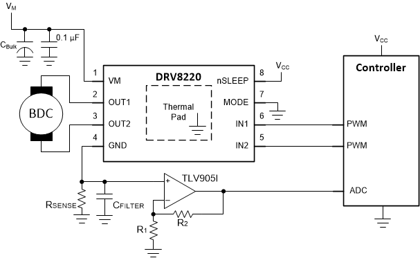
A small shunt resistor on the GND pin can provide current sense information back to the microcontroller ADC. The microcontroller can use this information to detect motor load conditions, such as stall. Figure 9-23 shows an example schematic using the DRL package. If better current sensing dynamic range is needed, an amplifier can be added as shown in Figure 9-24.

The DSG thermal pad may be connected to the board ground net or the GND pin/sense signal net.
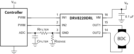
GUID-20200728-CA0I-9J1M-MXRB-GDBXGSDRRKRQ-low.gif Figure 9-23 Shunt resistor on GND pin of DRV8220 in the DRL package
GUID-20200728-CA0I-HH9D-PKDZ-06NJR1ZHRMCW-low.gif Figure 9-24 Current sense amplifier example