SLVSE38A April 2018 – July 2018 DRV8306
PRODUCTION DATA.
- 1 Features
- 2 Applications
- 3 Description
- 4 Revision History
- 5 Pin Configuration and Functions
- 6 Specifications
-
7 Detailed Description
- 7.1 Overview
- 7.2 Functional Block Diagram
- 7.3
Feature Description
- 7.3.1 Three Phase Smart Gate Drivers
- 7.3.2 DVDD Linear Voltage Regulator
- 7.3.3 Pulse-by-Pulse Current Limit
- 7.3.4 Hall Comparators
- 7.3.5 FGOUT Signal
- 7.3.6 Pin Diagrams
- 7.3.7 Gate-Driver Protective Circuits
- 7.4 Device Functional Modes
- 8 Application and Implementation
- 9 Power Supply Recommendations
- 10Layout
- 11Device and Documentation Support
- 12Mechanical, Packaging, and Orderable Information
Package Options
Mechanical Data (Package|Pins)
- RSM|32
Thermal pad, mechanical data (Package|Pins)
- RSM|32
Orderable Information
3 Description
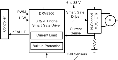
The DRV8306 device is an integrated gate driver for 3-phase brushless DC (BLDC) motor applications. The device provides three half-bridge gate drivers, each capable of driving high-side and low-side N-channel power MOSFETs. The DRV8306 device generates the proper gate drive voltages using an integrated charge pump for the high-side MOSFETs and a linear regulator for the low-side MOSFETs. The smart gate drive architecture supports up to 150-mA source and 300-mA sink peak gate drive current and 15-mA rms gate drive current capability.
The device provides an internal 120° commutation for the trapezoidal BLDC motor. The DRV8306 device has three Hall comparators which use the input from the Hall elements for internal commutation. The duty cycle ratio of the phase voltage of the motor can be adjusted through the PWM pin. Additional brake (nBRAKE) and direction (DIR) pins are provided for braking and setting the direction of the BLDC motor. A 3.3-V, 30-mA low-dropout (LDO) regulator is provided to supply the external controller and Hall elements. An additional FGOUT signal is provided which is a measure of the commutation frequency. This signal can be used for implementing the closed-loop control of BLDC motor.
A low-power sleep mode is provided to achieve low quiescent current draw by shutting down most of the internal circuitry. Internal protection functions are provided for undervoltage lockout, charge pump fault, MOSFET overcurrent, MOSFET short circuit, gate driver fault, and overtemperature. Fault conditions are indicated on the nFAULT pin.
Device Information(1)
| PART NUMBER | PACKAGE | BODY SIZE (NOM) |
|---|---|---|
| DRV8306 | VQFN (32) | 4.00 mm × 4.00 mm |
- For all available packages, see the orderable addendum at the end of the data sheet.
Simplified Schematic
