SBOS946 September 2020 INA848
PRODUCTION DATA
- 1 Features
- 2 Applications
- 3 Description
- 4 Revision History
- 5 Device Comparison Table
- 6 Pin Configuration and Functions
- 7 Specifications
- 8 Detailed Description
- 9 Application and Implementation
- 10Power Supply Recommendations
- 11Layout
- 12Device and Documentation Support
- 13Mechanical, Packaging, and Orderable Information
Package Options
Mechanical Data (Package|Pins)
- D|8
Thermal pad, mechanical data (Package|Pins)
Orderable Information
8.3.1 Topology
The INA848 is designed with TI's modern bipolar process that features super-beta input transistors.
Traditional bipolar transistors feature excellent voltage noise and offset drift, but suffer a tradeoff in high input bias current and high input bias current noise.
TI`s super-beta transistors offer the benefits of low voltage noise, low offset voltage drift with an additional improvement in reduction of the input bias current noise.
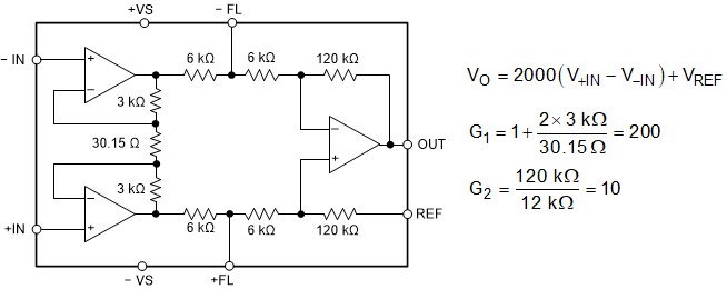
As shown in Figure 8-1, the INA848 is designed with a current feedback input stage that is optimized for high bandwidth in high gains. The device consists of three operational amplifiers configured at the front with a gain stage that integrates the gain resistor. This input stage preamplifies the differential input signal at a gain of 200. The output stage with the difference amplifier provides additional amplification of a gain of 10.
 Figure 8-1 Simplified Diagram of the INA848 With
Gain and Output Equations