SBOS946 September   2020 INA848

PRODUCTION DATA  

  1. Features
  2. Applications
  3. Description
  4. Revision History
  5. Device Comparison Table
  6. Pin Configuration and Functions
  7. Specifications
    1. 7.1 Absolute Maximum Ratings
    2. 7.2 ESD Ratings
    3. 7.3 Recommended Operating Conditions
    4. 7.4 Thermal Information
    5. 7.5 Electrical Characteristics
    6. 7.6 Typical Characteristics
  8. Detailed Description
    1. 8.1 Overview
    2. 8.2 Functional Block Diagram
    3. 8.3 Feature Description
      1. 8.3.1 Topology
      2. 8.3.2 Input Common-Mode Range
      3. 8.3.3 Input Protection
    4. 8.4 Device Functional Modes
  9. Application and Implementation
    1. 9.1 Application Information
      1. 9.1.1 Filter Pin
        1. 9.1.1.1 RC Filter Network
        2. 9.1.1.2 RLC Filter Network
      2. 9.1.2 Input Bias Current Return Path
    2. 9.2 Typical Application
      1. 9.2.1 Design Requirements
      2. 9.2.2 Detailed Design Procedure
        1. 9.2.2.1 Reference Pin
        2. 9.2.2.2 Noise Analysis
          1. 9.2.2.2.1 Reference Voltage Noise Contribution
      3. 9.2.3 Application Curves
  10. 10Power Supply Recommendations
  11. 11Layout
    1. 11.1 Layout Guidelines
    2. 11.2 Layout Example
  12. 12Device and Documentation Support
    1. 12.1 Documentation Support
      1. 12.1.1 Related Documentation
    2. 12.2 Receiving Notification of Documentation Updates
    3. 12.3 Support Resources
    4. 12.4 Trademarks
    5. 12.5 Electrostatic Discharge Caution
    6. 12.6 Glossary
  13. 13Mechanical, Packaging, and Orderable Information

Package Options

Mechanical Data (Package|Pins)
Thermal pad, mechanical data (Package|Pins)
Orderable Information

RLC Filter Network

In environments where a known, narrow-frequency band must be attenuated, a series LC filter network can be added between the filter pins, as shown in Figure 9-2. The connection adds to the internal resistor network, and results in a RLC filter network that is also commonly known as bandstop filter.

GUID-20200824-CA0I-XM9Q-TMP8-RDLC2S0QNDVS-low.svg Figure 9-2 Bandstop Filter

Use Equation 3 to calculate the middle frequency of the filter:

Equation 3. GUID-20200824-CA0I-FRZ0-DMXR-ZPZLBWW9LB4G-low.gif
In general, the width of the stopband is between one and two decades, meaning that the highest attenuation is between 10 to 100 around the middle frequency. This indication is commonly defined as the quality factor (Q factor) of the filter and is calculated by:
Equation 4. GUID-20200824-CA0I-KWD0-BQ4L-WVKHSCN9R5TH-low.gif

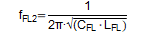
The resistor is given by the internal resistor of 6 kΩ; therefore, the damping factor of the filter can further be affected of the series resistance of the inductor LFL. For stable operation of the filter, choose an inductor in the range of 100 µH.