SBOS946 September 2020 INA848
PRODUCTION DATA
- 1 Features
- 2 Applications
- 3 Description
- 4 Revision History
- 5 Device Comparison Table
- 6 Pin Configuration and Functions
- 7 Specifications
- 8 Detailed Description
- 9 Application and Implementation
- 10Power Supply Recommendations
- 11Layout
- 12Device and Documentation Support
- 13Mechanical, Packaging, and Orderable Information
Package Options
Mechanical Data (Package|Pins)
- D|8
Thermal pad, mechanical data (Package|Pins)
Orderable Information
9.2.2.2 Noise Analysis
Low-noise instrumentation amplifiers such as the INA848 are designed to serve stringent and sensitive applications, such as surgical tools, microphones or other precision monitoring systems. A througough noise analysis is a key element in the design process.
TI`s super-beta transistors offer the benefits of low voltage noise and low current noise, thus allowing the INA848 excellent noise performance.
Figure 9-6 shows a simplified noise model including the gain stages of the INA848.
 Figure 9-6 Simplified Noise
Model
Figure 9-6 Simplified Noise
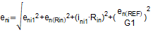
ModelTo get the total input-referred noise, eni, consider the source resistance seen by the positive and negative input pins of the instrumentation amplifier. The key elements that must be considered for a noise analysis in an instrumenation amplifier are:
- Current noise density ini1of the INA, see Section 7.5
- Voltage noise denisty eni1 of the INA, see Section 7.5
- Voltage noise density caused by source resistance ini× Rin
- Resistor noise from source resistance enRin , given by: √Rin × 4.04 nV/√Hz
- Reference voltage noise enref
The noise sources are uncorrelated
(that is, the noise signal is unpredictable). The result of mutliple uncorrelated
noise sources is the square root of the sum of their squares (RSS). Thus, the total
RTI noise density, eni, in
nV/√Hz can be derived from the following equation: