SBOS946 September 2020 INA848
PRODUCTION DATA
- 1 Features
- 2 Applications
- 3 Description
- 4 Revision History
- 5 Device Comparison Table
- 6 Pin Configuration and Functions
- 7 Specifications
- 8 Detailed Description
- 9 Application and Implementation
- 10Power Supply Recommendations
- 11Layout
- 12Device and Documentation Support
- 13Mechanical, Packaging, and Orderable Information
Package Options
Mechanical Data (Package|Pins)
- D|8
Thermal pad, mechanical data (Package|Pins)
Orderable Information
9.2.2.2.1 Reference Voltage Noise Contribution
Figure 9-7 shows the noise model of the reference buffer circuit given by Figure 9-5 using the OPA197 amplifier.
To compute the total noise for the reference buffer circuit, consider the thermal noise of the divider (that is a parallel network from noise perspective), the amplifier voltage noise (that is, enOPA = 5.5 nV/√Hz), and the voltage noise developed from the current noise of the amplifier (that is, inOPA = 1.5 fA/√Hz) through the divider.
 Figure 9-7 Reference Voltage Noise
Model
Figure 9-7 Reference Voltage Noise
ModelThus the total reference noise can be derived from following equation:
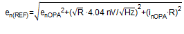
The reference noise is divided by the first gain stage of 200 at the INA848 to compute the input-referred noise. For reference noise less than 80 nV/√Hz, this contribution can be neglected in the analysis. The given example results in a total reference noise of 29 nV/√Hz, and thus is neglected.