SNVSC11 May 2022 LM25143-Q1
PRODUCTION DATA
- 1 Features
- 2 Applications
- 3 Description
- 4 Revision History
- 5 Description (continued)
- 6 Device Comparison Table
- 7 Pin Configuration and Functions
- 8 Specifications
-
9 Detailed Description
- 9.1 Overview
- 9.2 Functional Block Diagram
- 9.3
Feature Description
- 9.3.1 Input Voltage Range (VIN)
- 9.3.2 High-Voltage Bias Supply Regulator (VCC, VCCX, VDDA)
- 9.3.3 Enable (EN1, EN2)
- 9.3.4 Power-Good Monitor (PG1, PG2)
- 9.3.5 Switching Frequency (RT)
- 9.3.6 Clock Synchronization (DEMB)
- 9.3.7 Synchronization Out (SYNCOUT)
- 9.3.8 Spread Spectrum Frequency Modulation (DITH)
- 9.3.9 Configurable Soft Start (SS1, SS2)
- 9.3.10 Output Voltage Setpoint (FB1, FB2)
- 9.3.11 Minimum Controllable On Time
- 9.3.12 Error Amplifier and PWM Comparator (FB1, FB2, COMP1, COMP2)
- 9.3.13 Slope Compensation
- 9.3.14 Inductor Current Sense (CS1, VOUT1, CS2, VOUT2)
- 9.3.15 Hiccup Mode Current Limiting (RES)
- 9.3.16 High-Side and Low-Side Gate Drivers (HO1, HO2, LO1, LO2, HOL1, HOL2, LOL1, and LOL2)
- 9.3.17 Output Configurations (MODE, FB2)
- 9.4 Device Functional Modes
-
10Application and Implementation
- 10.1 Application Information
- 10.2
Typical Applications
- 10.2.1 Design 1 – 5-V and 3.3-V Dual-Output Buck Regulator for Automotive Applications
- 10.2.2 Design 2 – Two-Phase, 15-A, 2.1-MHz Single-Output Buck Regulator for Automotive ADAS Applications
- 10.2.3 Design 3 – Two-Phase, 50-A, 300-kHz Single-Output Buck Regulator for High-Voltage Automotive Battery Applications
- 11Power Supply Recommendations
- 12Layout
- 13Device and Documentation Support
- 14Mechanical, Packaging, and Orderable Information
Package Options
Mechanical Data (Package|Pins)
- RHA|40
Thermal pad, mechanical data (Package|Pins)
- RHA|40
Orderable Information
10.2.1.2.6 Input Capacitors
A power supply input typically has a relatively high source impedance at the switching frequency. Good-quality input capacitors are necessary to limit the input ripple voltage. As mentioned earlier, dual-channel interleaved operation significantly reduces the input ripple amplitude. In general, the ripple current splits between the input capacitors based on the relative impedance of the capacitors at the switching frequency.
- Select the input capacitors with sufficient voltage and RMS ripple current ratings.
- Worst case input ripple for a two-channel buck regulator typically corresponds
to when one channel operates at full load and the other channel is disabled or
operates at no load. Use Equation 41 to calculate
the input capacitor RMS ripple current assuming a worst-case duty-cycle
operating point of 50%. Equation 41.

- Use Equation 42 to find the required input
capacitance. Equation 42.
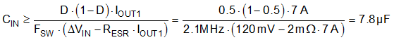
where
- ΔVIN is the input peak-to-peak ripple voltage specification.
- RESR is the input capacitor ESR.
- Recognizing the voltage coefficient of ceramic capacitors, select two 10-µF, 50-V, X7R, 1210 ceramic input capacitors for each channel. Place these capacitors adjacent to the relevant power MOSFETs.
- Use four 10-nF, 50-V, X7R, 0603 ceramic capacitors near each high-side MOSFET to supply the high di/dt current during MOSFET switching transitions. Such capacitors offer high self-resonant frequency (SRF) and low effective impedance above 100 MHz. The result is lower power loop parasitic inductance, thus minimizing switch-node voltage overshoot and ringing for lower EMI signature. Refer to Figure 12-2 in Section 12.1 for more detail.