SNVSC11 May   2022 LM25143-Q1

PRODUCTION DATA  

  1. Features
  2. Applications
  3. Description
  4. Revision History
  5. Description (continued)
  6. Device Comparison Table
  7. Pin Configuration and Functions
    1. 7.1 Wettable Flanks
  8. Specifications
    1. 8.1 Absolute Maximum Ratings
    2. 8.2 ESD Ratings
    3. 8.3 Recommended Operating Conditions
    4. 8.4 Thermal Information
    5. 8.5 Electrical Characteristics
    6. 8.6 Switching Characteristics
    7. 8.7 Typical Characteristics
  9. Detailed Description
    1. 9.1 Overview
    2. 9.2 Functional Block Diagram
    3. 9.3 Feature Description
      1. 9.3.1  Input Voltage Range (VIN)
      2. 9.3.2  High-Voltage Bias Supply Regulator (VCC, VCCX, VDDA)
      3. 9.3.3  Enable (EN1, EN2)
      4. 9.3.4  Power-Good Monitor (PG1, PG2)
      5. 9.3.5  Switching Frequency (RT)
      6. 9.3.6  Clock Synchronization (DEMB)
      7. 9.3.7  Synchronization Out (SYNCOUT)
      8. 9.3.8  Spread Spectrum Frequency Modulation (DITH)
      9. 9.3.9  Configurable Soft Start (SS1, SS2)
      10. 9.3.10 Output Voltage Setpoint (FB1, FB2)
      11. 9.3.11 Minimum Controllable On Time
      12. 9.3.12 Error Amplifier and PWM Comparator (FB1, FB2, COMP1, COMP2)
      13. 9.3.13 Slope Compensation
      14. 9.3.14 Inductor Current Sense (CS1, VOUT1, CS2, VOUT2)
        1. 9.3.14.1 Shunt Current Sensing
        2. 9.3.14.2 Inductor DCR Current Sensing
      15. 9.3.15 Hiccup Mode Current Limiting (RES)
      16. 9.3.16 High-Side and Low-Side Gate Drivers (HO1, HO2, LO1, LO2, HOL1, HOL2, LOL1, and LOL2)
      17. 9.3.17 Output Configurations (MODE, FB2)
        1. 9.3.17.1 Independent Dual-Output Operation
        2. 9.3.17.2 Single-Output Interleaved Operation
        3. 9.3.17.3 Single-Output Multiphase Operation
    4. 9.4 Device Functional Modes
      1. 9.4.1 Standby Modes
      2. 9.4.2 Diode Emulation Mode
      3. 9.4.3 Thermal Shutdown
  10. 10Application and Implementation
    1. 10.1 Application Information
      1. 10.1.1 Power Train Components
        1. 10.1.1.1 Buck Inductor
        2. 10.1.1.2 Output Capacitors
        3. 10.1.1.3 Input Capacitors
        4. 10.1.1.4 Power MOSFETs
        5. 10.1.1.5 EMI Filter
      2. 10.1.2 Error Amplifier and Compensation
    2. 10.2 Typical Applications
      1. 10.2.1 Design 1 – 5-V and 3.3-V Dual-Output Buck Regulator for Automotive Applications
        1. 10.2.1.1 Design Requirements
        2. 10.2.1.2 Detailed Design Procedure
          1. 10.2.1.2.1 Custom Design With WEBENCH® Tools
          2. 10.2.1.2.2 Custom Design With Excel Quickstart Tool
          3. 10.2.1.2.3 Inductor Calculation
          4. 10.2.1.2.4 Current-Sense Resistance
          5. 10.2.1.2.5 Output Capacitors
          6. 10.2.1.2.6 Input Capacitors
          7. 10.2.1.2.7 Compensation Components
        3. 10.2.1.3 Application Curves
      2. 10.2.2 Design 2 – Two-Phase, 15-A, 2.1-MHz Single-Output Buck Regulator for Automotive ADAS Applications
        1. 10.2.2.1 Design Requirements
        2. 10.2.2.2 Detailed Design Procedure
        3. 10.2.2.3 Application Curves
      3. 10.2.3 Design 3 – Two-Phase, 50-A, 300-kHz Single-Output Buck Regulator for High-Voltage Automotive Battery Applications
        1. 10.2.3.1 Design Requirements
        2. 10.2.3.2 Detailed Design Procedure
        3. 10.2.3.3 Application Curves
  11. 11Power Supply Recommendations
  12. 12Layout
    1. 12.1 Layout Guidelines
      1. 12.1.1 Power Stage Layout
      2. 12.1.2 Gate-Drive Layout
      3. 12.1.3 PWM Controller Layout
      4. 12.1.4 Thermal Design and Layout
      5. 12.1.5 Ground Plane Design
    2. 12.2 Layout Example
  13. 13Device and Documentation Support
    1. 13.1 Device Support
      1. 13.1.1 Third-Party Products Disclaimer
      2. 13.1.2 Development Support
        1. 13.1.2.1 Custom Design With WEBENCH® Tools
    2. 13.2 Documentation Support
      1. 13.2.1 Related Documentation
        1. 13.2.1.1 PCB Layout Resources
        2. 13.2.1.2 Thermal Design Resources
    3. 13.3 Receiving Notification of Documentation Updates
    4. 13.4 Support Resources
    5. 13.5 Trademarks
    6. 13.6 Electrostatic Discharge Caution
    7. 13.7 Glossary
  14. 14Mechanical, Packaging, and Orderable Information

Package Options

Mechanical Data (Package|Pins)
Thermal pad, mechanical data (Package|Pins)
Orderable Information
Compensation Components

Choose compensation components for a stable control loop using the procedure outlined as follows.

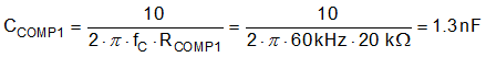
  1. Based on a specified open-loop gain crossover frequency, fC, of 60 kHz, use Equation 43 to calculate RCOMP1, assuming an effective output capacitance of 130 µF. Select RCOMP1 of 20 kΩ.
    Equation 43. GUID-77450265-4D0C-4744-A329-8A7ACC46F4D0-low.gif
  2. Calculate CCOMP1 to create a zero at the higher of (1) one tenth of the crossover frequency, or (2) the load pole. Select a CCOMP1 capacitor of 1 nF.
    Equation 44. GUID-7E8C2EDC-C6BD-4512-8DFF-7BC712F25366-low.gif
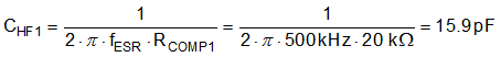
  3. Calculate CHF1 to create a pole at the ESR zero and to attenuate high-frequency noise at COMP. Select a CHF1 capacitor of 15 pF.
    Equation 45. GUID-50A247B8-51E8-40F6-96AA-1EFAF1D334C4-low.gif
Note:

Set a fast loop with high RCOMP and low CCOMP values to improve the response when recovering from operation in dropout.