SNVS603D August 2009 – July 2019 LM3424
PRODUCTION DATA.
- 1 Features
- 2 Applications
- 3 Description
- 4 Revision History
- 5 Pin Configuration and Functions
- 6 Specifications
-
7 Detailed Description
- 7.1 Overview
- 7.2 Functional Block Diagram
- 7.3
Feature Description
- 7.3.1 Current Regulators
- 7.3.2 Peak Current Mode Control
- 7.3.3 Average LED Current
- 7.3.4 Thermal Foldback and Analog Dimming
- 7.3.5 Current Sense and Current Limit
- 7.3.6 Slope Compensation
- 7.3.7 Control Loop Compensation
- 7.3.8 Start-Up Regulator and Soft-Start
- 7.3.9 Overvoltage Lockout (OVLO)
- 7.3.10 Input Undervoltage Lockout (UVLO)
- 7.3.11 PWM Dimming
- 7.3.12 Thermal Shutdown
- 7.4 Device Functional Modes
-
8 Application and Implementation
- 8.1 Application Information
- 8.2
Typical Applications
- 8.2.1
Basic Topology Schematics
- 8.2.1.1 Design Requirements
- 8.2.1.2
Detailed Design Procedure
- 8.2.1.2.1 Operating Point
- 8.2.1.2.2 Switching Frequency
- 8.2.1.2.3 Average LED Current
- 8.2.1.2.4 Thermal Foldback
- 8.2.1.2.5 Inductor Ripple Current
- 8.2.1.2.6 LED Ripple Current
- 8.2.1.2.7 Peak Current Limit
- 8.2.1.2.8 Slope Compensation
- 8.2.1.2.9 Loop Compensation
- 8.2.1.2.10 Input Capacitance
- 8.2.1.2.11 NFET
- 8.2.1.2.12 Diode
- 8.2.1.2.13 Output OVLO
- 8.2.1.2.14 Input UVLO
- 8.2.1.2.15 Soft-Start
- 8.2.1.2.16 PWM Dimming Method
- 8.2.1.2.17 Analog Dimming Method
- 8.2.2
Buck-Boost Application
- 8.2.2.1 Design Requirements
- 8.2.2.2
Detailed Design Procedure
- 8.2.2.2.1 Operating Point
- 8.2.2.2.2 Switching Frequency
- 8.2.2.2.3 Average LED Current
- 8.2.2.2.4 Thermal Foldback
- 8.2.2.2.5 Inductor Ripple Current
- 8.2.2.2.6 Output Capacitance
- 8.2.2.2.7 Peak Current Limit
- 8.2.2.2.8 Slope Compensation
- 8.2.2.2.9 Loop Compensation
- 8.2.2.2.10 Input Capacitance
- 8.2.2.2.11 NFET
- 8.2.2.2.12 Diode
- 8.2.2.2.13 Input UVLO
- 8.2.2.2.14 Output OVLO
- 8.2.2.2.15 Soft-Start
- 8.2.2.3 Application Curve
- 8.2.3 Boost Application
- 8.2.4 Buck-Boost Application
- 8.2.5 Boost Application
- 8.2.6 Buck-Boost Application
- 8.2.7 Buck Application
- 8.2.8 Buck-Boost Application
- 8.2.9 SEPIC Application
- 8.2.1
Basic Topology Schematics
- 9 Power Supply Recommendations
- 10Layout
- 11Device and Documentation Support
- 12Mechanical, Packaging, and Orderable Information
Package Options
Mechanical Data (Package|Pins)
- PWP|20
Thermal pad, mechanical data (Package|Pins)
- PWP|20
Orderable Information
8.2.2.2.9 Loop Compensation
ωP1 is approximated:
Equation 129. 

ωZ1 is approximated:
Equation 130. 

TU0 is approximated:
Equation 131. 

To ensure stability, calculate ωP2:
Equation 132. 

Solve for CCMP:
Equation 133. 

To attenuate switching noise, calculate ωP3:
Equation 134. 

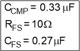
Assume RFS = 10Ω and solve for CFS:
Equation 135. 

The chosen components from step 9 are:
Equation 136. 
